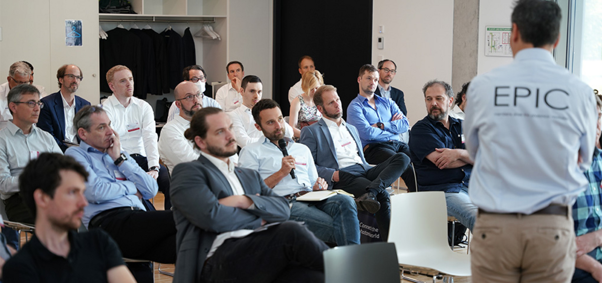
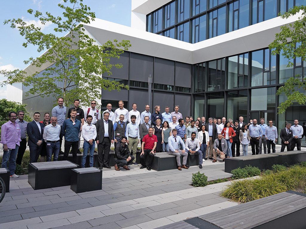
Last week, more than 50 experts, leading representatives and multiplicators in the microoptics and photonics industries met at Nanoscribe’s headquarters in the Zeiss Innovation Hub @KIT in Karlsruhe were the European Photonics Industry Consortium (EPIC) together with Nanoscribe invited to the EPIC Meeting “Advanced Microoptics: Simulation, Fabrication & Characterization”. The in total 17 talks and three keynote presentations outlined the entire supply chain in microoptics from design tools, rapid prototyping and metrology to fabrication and scaling it up to mass manufacturing.
Challenges in design and fabrication of advanced microoptics applications
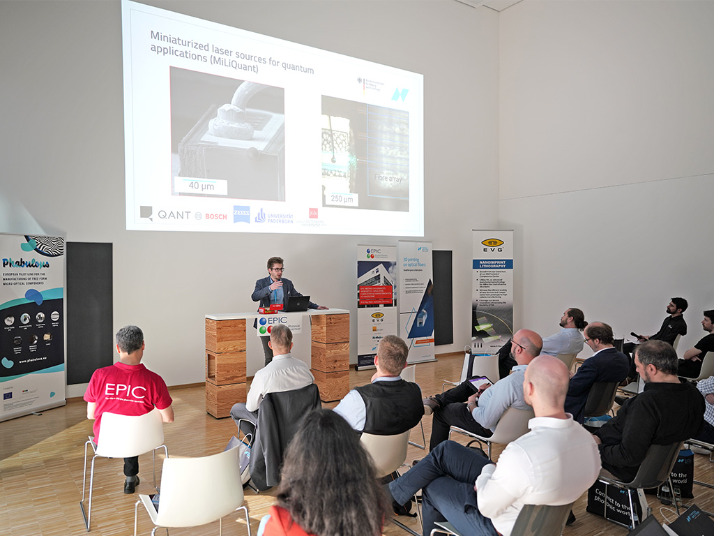
The two sessions on the first conference day offered various in-depth insights into the design and simulation of advanced microoptical systems as well as microfabrication technologies for refractive and diffractive microoptics. Both sessions started with a keynote, one of which was by Chief Science Officer (CSO) and co-founder of Nanoscribe Dr. Michael Thiel on the benefits of additive manufacturing technologies such as Two-Photon Grayscale Lithography (2GL ®) for prototyping and mastering of advanced microoptics as well as serial fabrication of microoptical coupling elements in photonics packaging. The talks outlined the fabrication of refractive and diffractive microoptical applications, also focusing on 3D microoptics, freeform microlenses, metalenses, wafer-scale manufacturing, and potential applications in many fields such as nanophotonics, lasers and endoscopy.
Replication process chains to scale up microoptics manufacturing
Another challenge in microoptics manufacturing is the upscaling to mass production. Replication technologies are a key element and important pathway in this process. Well-known replication technologies such as nanoimprint lithography (NIL), injection molding and monolithic molding were discussed in the presentations of the two sessions on the second conference day. In this context, Nanoscribe partners with EV Group and kdg opticomp for offering proven and reliable process chains by combining 2GL-based mastering of microoptics with NIL and injection molding to replicate them. Further discussions in these panel sessions were focused on the challenges in manufacturing and mass production of advanced microoptics such as freeform lenses and metalenses. Moreover, the sessions focused on characterization of microoptics and inline metrology.
Insights into Nanoscribe’s microfabrication solutions and systems
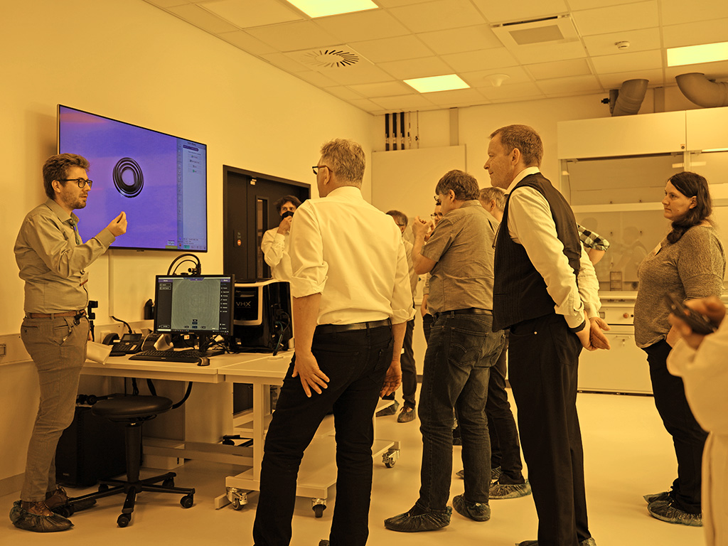
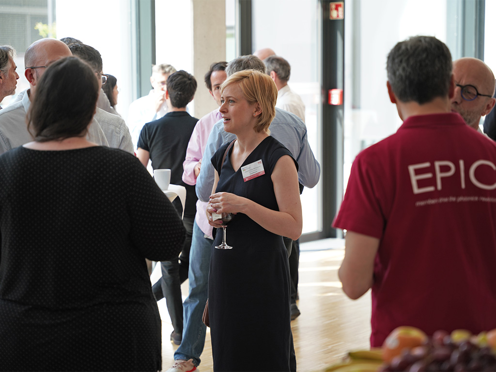
One of our highlights was to show all attendees around in our Microfabrication Experience Center to introduce them to our high-precision additive manufacturing technologies. During a guided tour in our showroom and Demolab, there were many opportunities to marvel at innovative microoptical applications and exchange ideas on how to benefit from additive manufacturing technologies in the rapid prototyping and manufacturing of highly sophisticated microoptical applications.
More about Nanoscribe’s microfabrication technologies
If you would also like to learn more about our microfabrication technologies and application opportunities, then we recommend to have a look into our premium resources. Alongside on-demand webinars, in our premium resources section we offer you whitepapers on Two-Photon Polymerization (2PP) and Two-Photon Grayscale Lithography (2GL ®), exclusive data and fact sheets for Nanoscribe printers and photoresins. Moreover, via a keyword-underpinned database you find hundreds of scientific publications of our customers in your specific application area.