Press release
April 16, 2021

Photonic packaging to boost information processing capacity in optical computing 

Breaking Moore’s Law: New photonic computing project PHOENICS aims to speed up artificial intelligence computing power to petascale processing levels

Münster/Karlsruhe. Nanoscribe is project partner in the EU-funded photonic computing project PHOENICS. The 4-year project that is coordinated by the University of Münster (Germany) brings together world leaders in neuromorphic photonic computing to achieve energy-efficient petascale processing power with ultra-high bandwidth. The aim is to develop disruptive methods for implementing next-generation computing platforms for applications in artificial intelligence (AI).

Visualization of chip-to-chip coupling

Applications employing artificial intelligence (AI) pose enormous challenges for electronic hardware in terms of computing power and storage capacity. AI needs processing power growing at a rate of more than five times higher than given by Moore’s Law and this is not possible with current electronic approaches. The PHOENICS project aims to address these challenges with innovative hardware approaches for processing the enormous data volumes, which are needed by demanding AI applications. By moving away from electronic towards photonic approaches, the PHOENICS project will establish disruptive methods for ultrafast information processing.

Photonic integration of different chip platforms

PHOENICS stands for “Photonic enabled petascale in-memory computing with femtojoule energy consumption” and sums up the three goals of the project: In contrast to traditional hardware, the concept of in-memory computing will allow data processing more similar to the human brain by removing the separation between computing and data storage units; photonic technology provides high speed data transport where current electronic systems face severe limitations; taken together, this will lead to a significant reduction of the energy demand.

The PHOENICS information processing architecture is based on the hybrid integration of three different chip platforms: a frequency microcomb chip, which is developed jointly by EPFL and MicroR Systems, an InP (indium phosphide) active modulation unit developed by HHI, complemented with a silicon photonics processor developed by the Universities of Exeter, Oxford, and Ghent. The University of Münster, Nanoscribe and IBM will design the system architecture and join the chip platforms.

Advances in alignment and packaging of photonic components

In PHOENICS, Nanoscribe will develop new hardware- and software-based solutions for photonic packaging. A key challenge for the industrialization of photonically packaged systems is the wide variety of different photonic platforms which typically all have different optical coupling interfaces. Efficient optical coupling without active alignment thus becomes almost impossible. Nanoscribe intends to integrate the results of the project into complete photonic packaging solutions consisting of automated systems, software, photoresins, and corresponding processes.

Nanoscribe will deploy the maskless lithography system Quantum X as its hardware framework and is collaborating to establish an advanced platform as the industry standard for next-generation photonic packaging.

Multidisciplinary EU-funded project

PHOENICS brings together 9 leading research institutes and companies. The 4-year project is a joint research effort of the coordinating University of Münster (Germany) in collaboration with University of Exeter (UK), École polytechnique fédérale de Lausanne (EPFL, Switzerland), Nanoscribe (Germany), University of Oxford (UK), Heinrich Hertz Institute of the Fraunhofer Gesellschaft (HHI, Germany), Ghent University (Belgium), IBM Research GmbH (Switzerland) and MicroR Systems (Switzerland).

The project has been awarded a grant of EUR 5.8 million from Horizon 2020, the EU program for research and innovation. Over the 4-year funding period, the consortium plans to establish photonic computing as a competitive approach for machine learning.

About Nanoscribe

The medium-sized company develops and produces 3D printers and maskless lithography systems for microfabrication as well as specially developed printing materials and application-specific solution sets. The specialist for additive manufacturing of high-precision structures and objects on the nano-, micro- and mesoscale was founded in 2007 as a spin-off of the Karlsruhe Institute of Technology (KIT). With the Carl Zeiss AG (ZEISS), Nanoscribe has a strong partner and investor at its side. Today, with more than 70 employees and subsidiaries in China and the USA, Nanoscribe has become the market and technology leader. More than 2,000 users and operators at top universities and innovative industrial companies worldwide benefit from the groundbreaking technology and application tailored solutions for 3D Microfabrication.
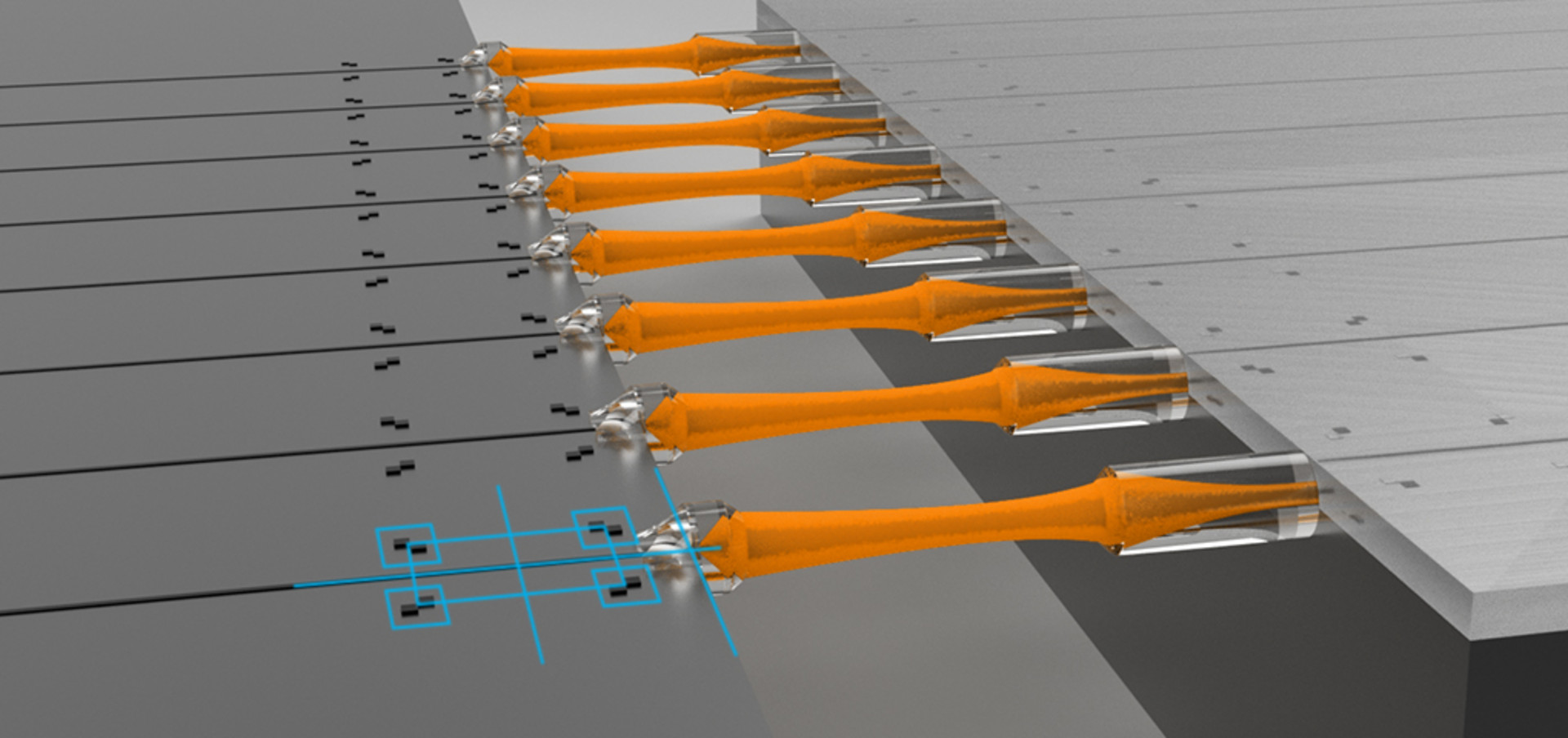
Caption

Img. 1: Visualization of chip-to-chip coupling for photonic packaging with automated alignment. Image: T. Hoose, Nanoscribe

Right of use and media relations

Our image may be used free of charge for editorial purposes. Please state the source as follows: "Image: Nanoscribe, www.nanoscribe.com". The image must not be used for commercial purposes or passed on to third parties.
In case of questions or if you would like to be added to our press mailing list, please do not hesitate to contact Dr. Alena Kirchenbauer, media@nanoscribe.com.

Stay up to date with our latest press releases about Nanoscribe and the world of 3D Microfabrication. Directly get in touch with us to discuss further press activities: Media relations

Login Register
Contact us
Close

It's your choice

Cookies help us to better understand you as a visitor and to provide you with a better experience.

It's your choice
Cookies help us to better understand you as a visitor and to provide you with a better experience.
Legal Notice Privacy Policy
Accept all Individual Settings