Aligned 2-Photon Lithography (A2PL®) for photonics packaging
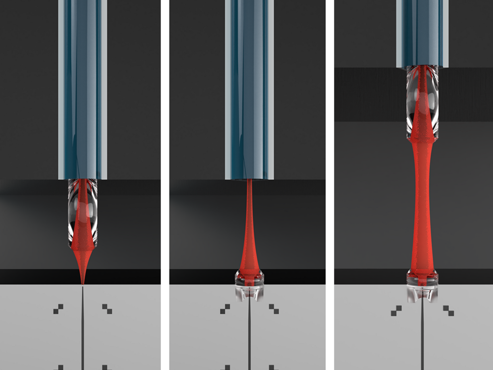
To fabricate efficient optical interconnects for photonic integration, or for miniaturized imaging optics, freeform microoptics can be printed directly onto optical fibers or photonic chips with submicron accuracy, provided by our A2PL microfabrication solution with highest resolution 3D printing and nanoprecision 3D alignment.
Photonics packaging and aligned 3D printing solutions
Optoelectronic components and modules based on photonic integrated circuits (PICs) are on the rise. They are increasingly incorporated into devices for medical sensing, LiDAR systems or quantum computing. This requires industrial solutions for an efficient photonics packaging, which is associated with technical challenges.
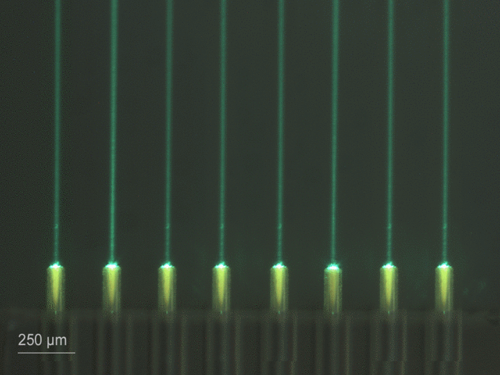
The concept of Free Space Microoptical Coupling (FSMOC), realized with 3D-printed microoptical elements precisely 3D-aligned on the facet of optical fibers or on photonic chips, provides a robust and efficient solution for coupling light into photonic chips or to other fiber arrays. These high-precision microoptics either focus or collimate the exceeding light beam of optical fibers or photonic chips onto the facet of photonic chips, enabling mode field conversions or light coupling over distances of up to millimeters.
The A2PL technology in the high-performance 3D printer Quantum X align is designed for manufacturing freeform microoptics automatically aligned on predefined positions for FSMOC applications. The printer’s automatic 3D fiber core detection system and automatic tilt correction guarantee alignment with nanoprecision and highest shape accuracy when printing onto photonic chips, single cleaved fibers or v-groove fiber arrays. 3D-printed microoptics have several advantages over traditional lensed or tapered fibers. Complete control over design parameters of freeform microlenses enables aspheric and asymmetric designs to correct for various aberrations and tailor the beam profile to match almost any coupling application.
Deep insights into integrated photonics
for data communication
A new publication “Integrated Photonics for Data Communication Applications” has been published by Elsevier. The book introduces readers to the key concepts and design principles of integrated photonics. It also provides an overview of key performance metrics and manufacturing methods from advanced photonic devices to integrated photonic circuits.
In Chapter 12.9, Jörg Smolenski, Business Development Manager at Nanoscribe together with Professor Wolfram Pernice and Helge Gehring from the University of Münster present the process principles and applications of the 3D printing of microoptics on dies for integrated photonics, such as tapers, lenses, and free space microoptical couplers.
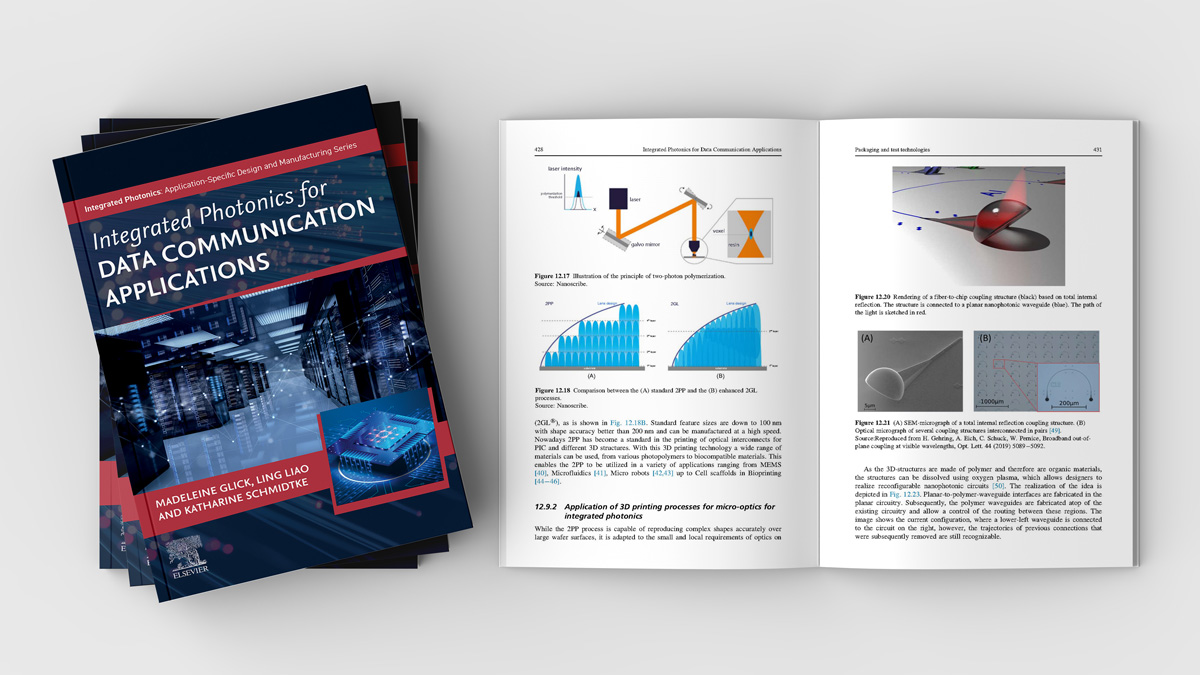
The chapter explains the working principle of Two-Photon Polymerization (2PP) and the enhanced and advantageous printing process of Two-Photon Grayscale Lithography (2GL®) for the fabrication of microoptics. It also offers application scenarios where fiber-to-chip coupling structures come into play and provides an outlook on future developments in photonics packaging.
Integrated Photonics for Data Communication Applications
Madeleine Glick, Ling Liao and Katharine Schmidtke
Connect to the photonic world

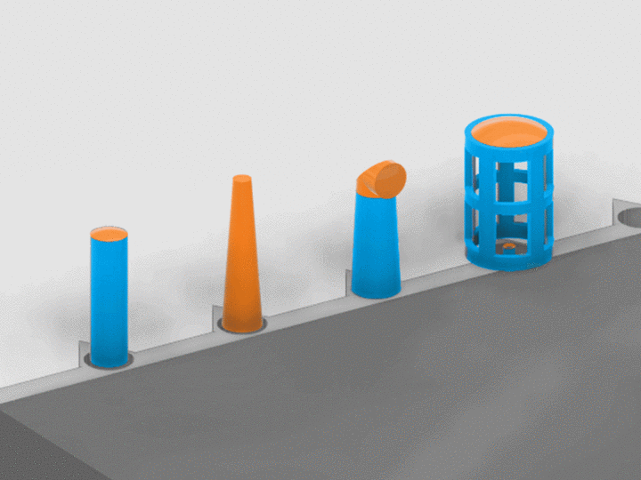
Integrated photonics
application opportunities
Looking to assess the opportunities for your integrated photonics and photonics packaging project? Explore the application options of our 3D Microfabrication solutions and view the 10 most recent scientific publications in materials engineering from over 1,800 peer-reviewed journal articles.
To view the details of the publications and to find more research topics and applications in which Nanoscribe 2PP-based 3D printing systems are already successfully used, just enter our premium resources – log in or register for free.
View more innovation projects
You get more publication examples and deeper insights within our premium resources. Via a keyword-underpinned database you find more than 1,800 scientific publications of our customers in specific application areas. Make use of the tool to gather valuable know-how and background information about the manifold application options.


