News
May 16, 2019

Successful installation of 1st Photonic Professional GT2 at KEIO University

Researchers at Keio University standing at a Nanoscribe Photonic Professional GT2 system
LTR: Prof. Dr. Kotaro Oka, Dep. of Biosciences and Informatics/ Prof. Dr. Keiya Shirahama, Faculty of Science and Technology/ Ryosuke Terada, Central Service Facilities for Research/ Hayato Tsuruta, Japan Laser Corp./ Tomoaki Mitani, Central Service Facilities for Research

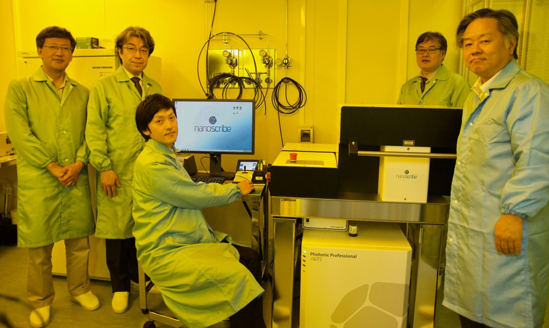
Back to the roots: KEIO University in Japan is now proud owner of a Photonic Professional GT2 system. The first installation of our latest 3D printer model could be considered a journey back to the starting point of the technology of two-photon polymerization (2PP). In 1997 Professor Satoshi Kawata provided the experimental proof of two-photon-polymerization in Japan. Nanoscribe utilizes 2PP’s strength to expose photoresists with extreme focus and highest resolution for the direct fabrication of nano- and microstructures that are otherwise impossible to produce.

“Both, the School of Medicine and the Faculty of Science and Technology, will have access to this powerful microfabrication tool”, Mr. Tomoaki Mitani, manager at Central Service Facilities for Research, explained after the successful installation. The range of possible applications extends from the printing of microchannels for electrochemical sensors to the development of novel optical elements and tissue engineering research in 3D cultures.

Our CEO Martin Hermatschweiler is pleased that users at KEIO can now realize pioneering ideas that were beyond their reach before. Nowadays, more than 180 Nanoscribe systems around the globe are used for various applications in science and industry. “And our user community is steadily growing due to a large number of multi-user facilities”, Hermatschweiler underlines.

Relaunched in December 2018, the model Photonic Professional GT2 pushes the boundaries of nano- and microfabrication offering new solutions for additive manufacturing and maskless lithography. Thanks to optimized hardware and software components as well as new printing materials specially developed for larger volumes, high-resolution microstructures up to a height of 8 mm can now be produced for the first time. While Nanoscribe devices have always been optimally suited to the additive production of the finest structures, objects with submicrometer details from typically 160 nanometers up to the millimeter range on a printing area of up to 100x100 mm² can now be produced in a very short time.

Login Register
Contact us
Close

It's your choice

Cookies help us to better understand you as a visitor and to provide you with a better experience.

It's your choice
Cookies help us to better understand you as a visitor and to provide you with a better experience.
Legal Notice Privacy Policy
Accept all Individual Settings