

Fiber-to-chip coupling
Plug-and-play connector for highly efficient and scalable coupling
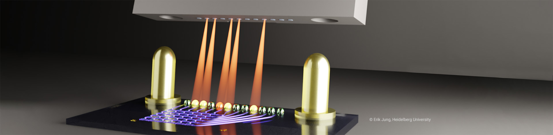
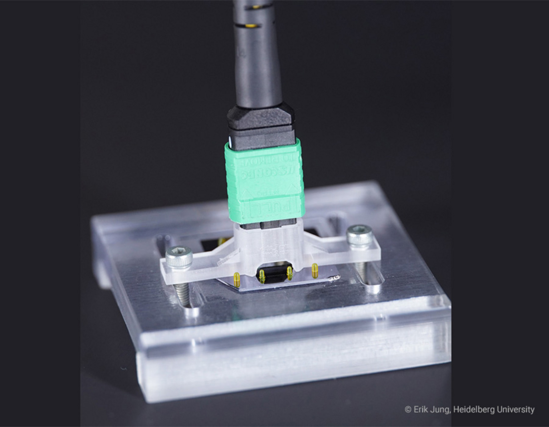
Researchers at Heidelberg University have developed a scalable plug-and-play fiber-to-chip connector fabricated using aligned, high-precision 3D printing. The approach enables self-aligned, broadband, low-loss optical coupling, replacing complex active-alignment setups with a simple insertion-locked connection, fabricated in under three minutes packaging time per port.
The demonstrated solution achieves self-aligned fiber coupling with sub-dB insertion losses and nearly wavelength-independent performance. This novel packaging concept leverages aligned 3D printing to combine optical coupling and mechanical alignment, paving the way for scalable, alignment-free photonics packaging in PIC-based systems.
Facts & figures
The plug-and-play connector solution consists of:
-
Focusing total internal reflection (TIR) couplers
-
Millimeter-high alignment pins
Print parameters:
-
TIR couplers: SF Print Set (nanoscale details), photoresin IP-Dip2, and print time < 1 min per port
-
Alignment pins: LF Print Set (millimeter parts), photoresin IPX-Q
-
Packaging time: < 3 min per port
Key benefits of high-resolution, aligned 3D printing
-
On-chip printing with nanometer-level 3D alignment with detection accuracy down to ≤ 100 nm
-
Automatic detection, alignment and printing
-
Multi-scale 3D printing of optical and mechanical structures in a 2-step workflow

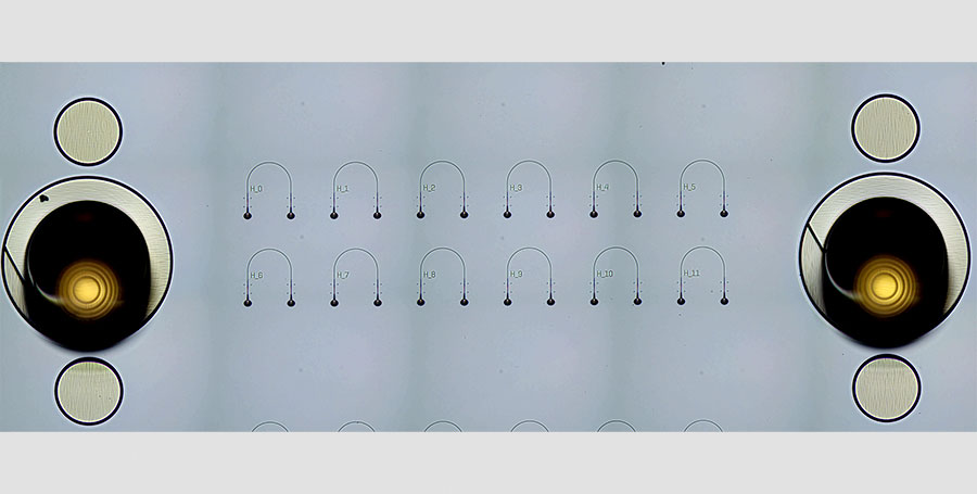

Scale up optics manufacturing with high-resolution 3D printing and automated alignment on fibers, chips, and wafers – enabling reliable, low-loss photonic coupling as well as sensing and imaging applications.