Scaling photonic computing
Explore photonic computing, emerging scaling concepts and high-performance photonic coupling in this webinar.
More infoPrinting freeform micro-optics on fibers, photonic chips, and wafers simplifies optical coupling, reduces assembly complexity, and streamlines production processes.
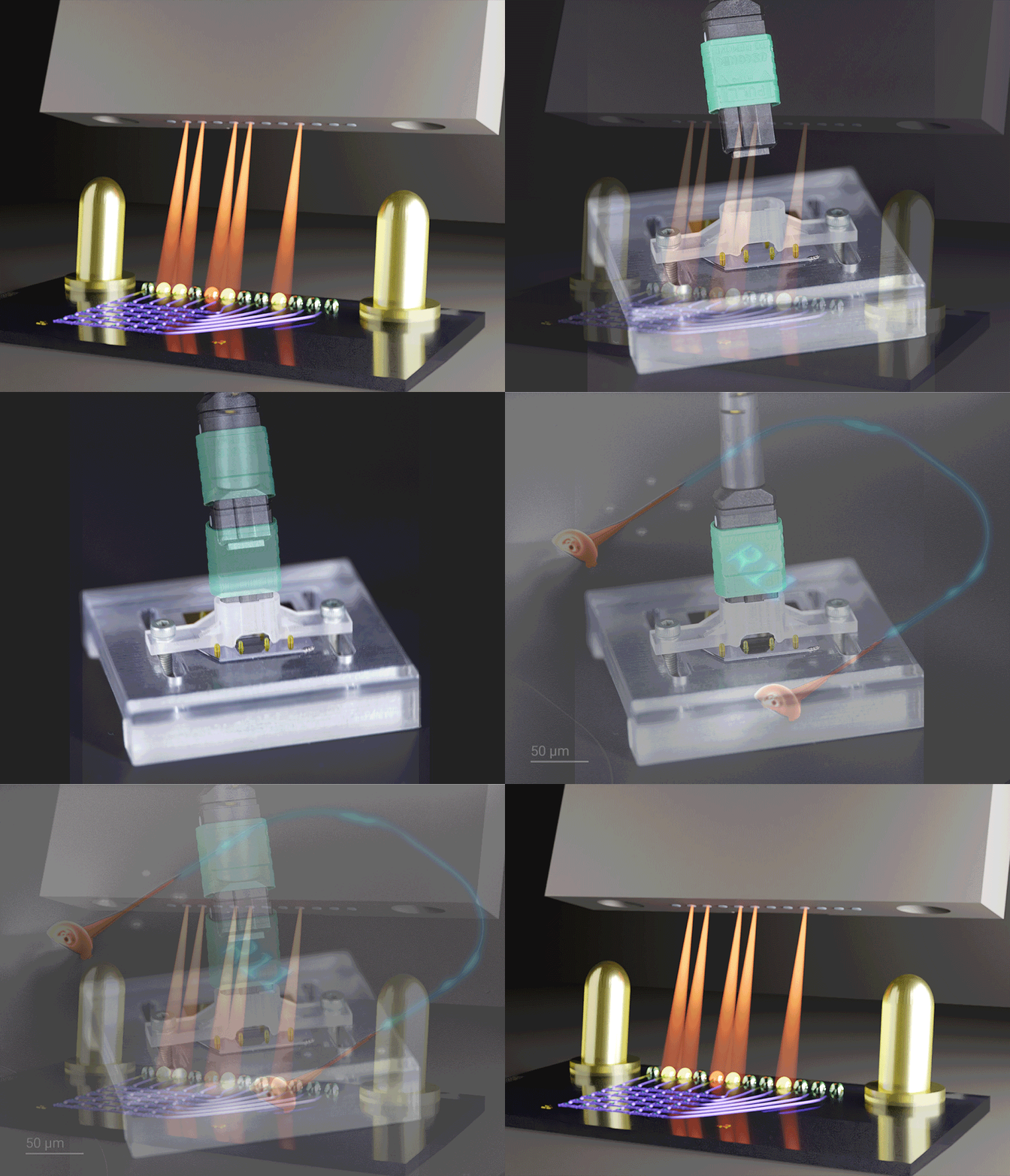
As photonic integrated circuits (PICs) move into high-volume manufacturing, packaging, alignment, and testing increasingly dominate manufacturing cost, throughput and yield. In many photonic products, packaging represents the largest share of total manufacturing cost.
The rapid growth of AI is driving unprecedented bandwidth and power demands, accelerating the adoption of optical interconnects and co-packaged optics (CPO). By integrating optical functions closer to compute, CPO can increase bandwidth density while reducing latency and energy consumption.
Yet optical packaging remains a major bottleneck. Precise alignment is required to secure low-loss optical coupling between fibers, lasers, and PICs, often at submicron tolerances. The industry's fragmented landscape has produced many highly specialized point solutions, driving complexity, investment requirements, and cost while suffering from low yield.
Scalable optical manufacturing therefore requires standardized, reliable coupling and packaging approaches that reduce alignment effort, lower costs, and accelerate market adoption.
| Interface diversity | Alignment efforts | Packaging economics | Time to market |
| Hybrid photonic architectures require versatile, low-loss coupling solutions across diverse interfaces. | Complex active alignment increases cycle times, limits throughput, and drives manufacturing costs. | Fragmented, application-specific solutions add complexity, capital intensity, and total cost of ownership. | Lengthy design iteration cycles slow product development, delay commercial deployment and return on investment (ROI). |

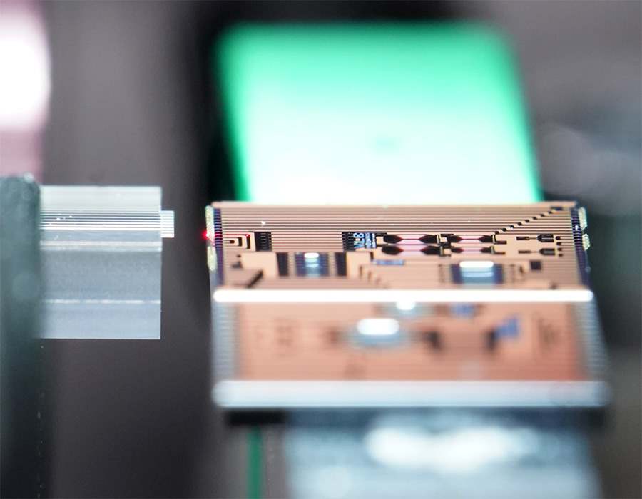
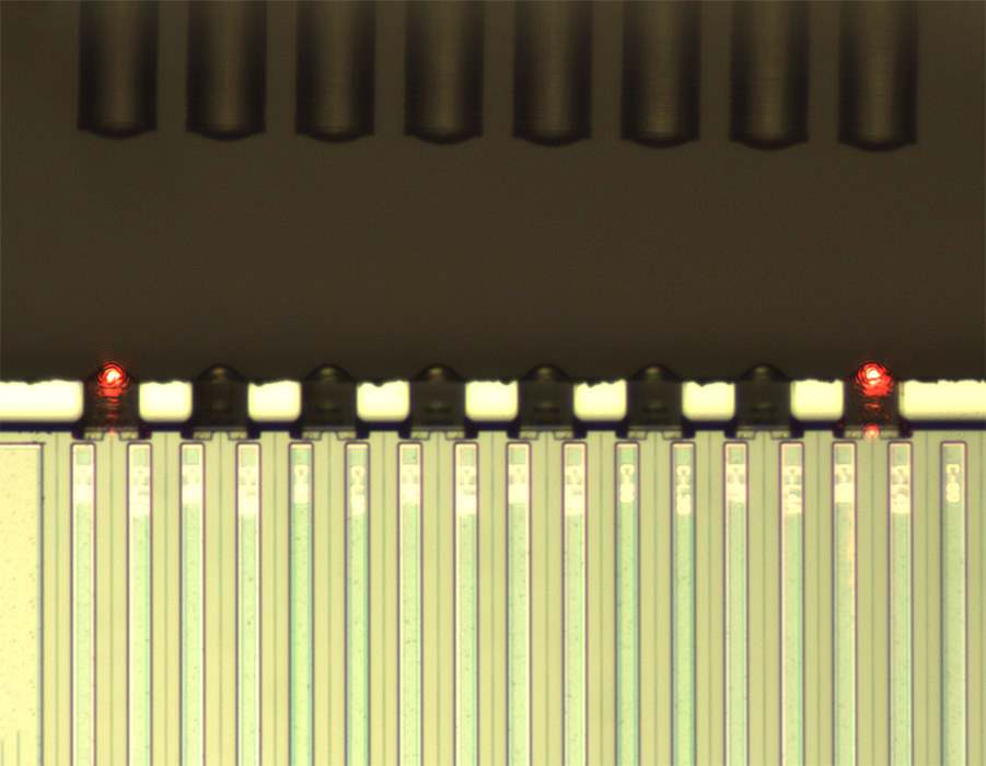
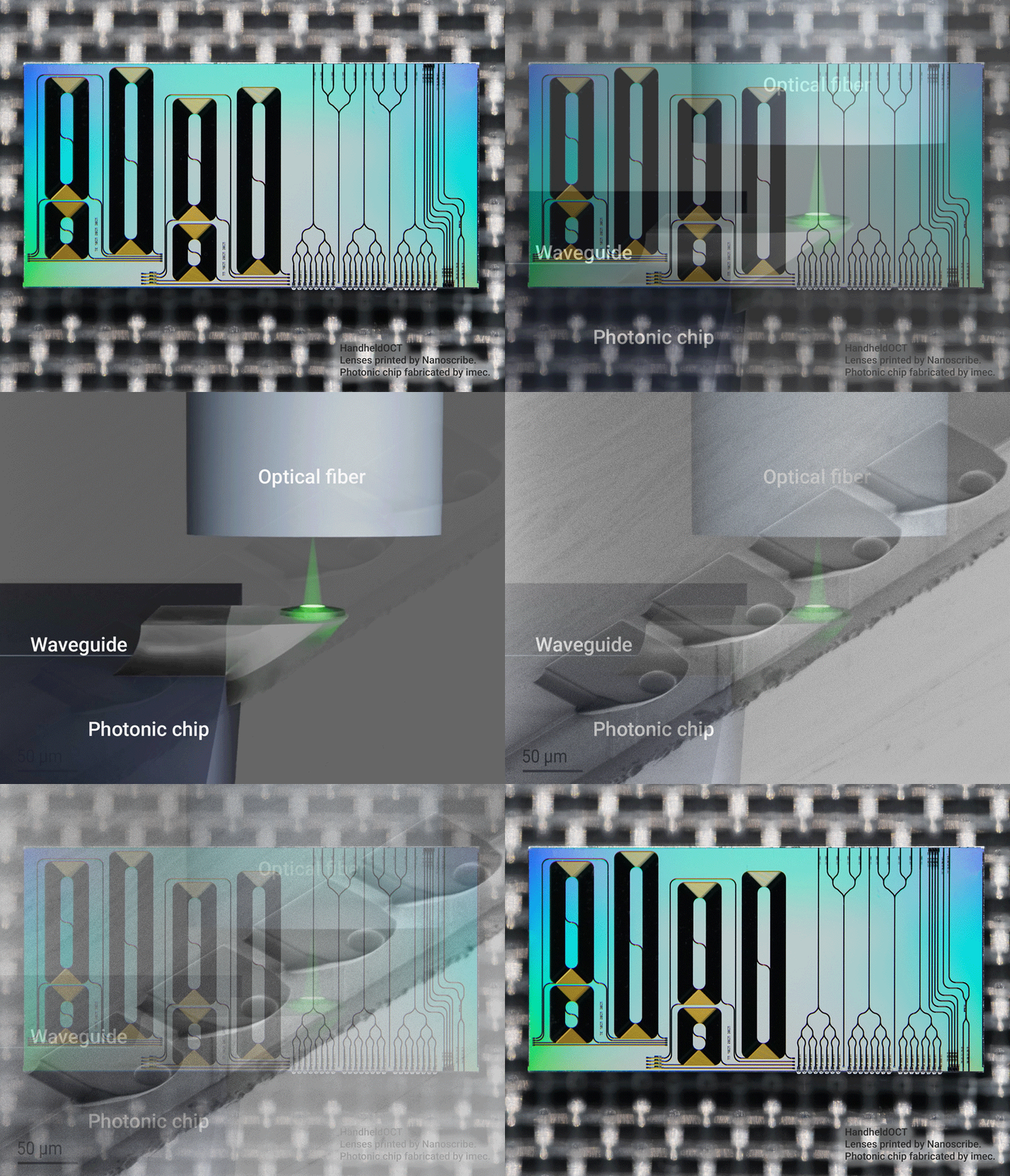
Nanoscribe addresses the photonic packaging challenges by fabricating optical couplers directly where they are needed: on fibers, chips, wafers, and photonic devices. Fiber cores, chip edges, fiducials, and surface features are automatically detected before printing of the optical interface in its precisely aligned position. This direct manufacturing approach combines alignment and fabrication in one workflow and vastly reduces assembly and testing efforts.
All types of coupling challenges are supported, including fiber-to-chip, edge and vertical coupling, as well as lensed fiber arrays.
3D-printed freeform micro-optics provide tailored beam shaping and mode-field adaptation, reducing insertion loss while increasing alignment tolerance and packaging robustness. By replacing multiple specialized point solutions with a versatile manufacturing platform, Nanoscribe helps lower packaging costs, shorten development cycles, and accelerate the adoption of next-generation photonic and co-packaged optical (CPO) systems.
| Digital manufacturing | Automated alignment | Versatile coupling | Freeform beam shaping |
| Save costs by replacing active alignment-based assembly of miniature components by versatile aligned 3D printing. | Print optical couplers on fiber facets, chip edges, and on-chip fiducials with alignment accuracies down to 100 nm. | One solution for printing of optics on fibers, at chip edges, on wafer surfaces, on active and passive devices | Secure low-loss optical coupling by mode field matching; print lenses for collimation and focusing, periscopes and beam-shaping optics. |
For industrial players evaluating 3D printing using Aligned 2-Photon Lithography (A2PL®) for PIC packaging, the question is no longer whether it can be fabricated. The key question is whether it can be integrated into a reliable, cost-efficient, high-yield packaging process for mass production. Nanoscribe combines aligned 3D microfabrication with streamlined developments to support the transition from fabricating prototypes via small series production to scaled manufacturing. For photonics packaging houses, OSATs, foundries, and hyperscalers, we offer turnkey process-line solutions tailored to specific integration and production requirements.
Lower assembly complexity
Reduce component count and assembly effort by 3D printing of optical couplers directly at the interfaces.
Relaxed tolerances
Enable robust, low-cost passive alignment through tailored beam shaping and mode-field adaptation.
Fast iteration cycles
Go from design update to printed prototype in under 24 hours, without tooling, masks, or fabrication delays.
Dies and wafers
Integrate optical couplers at any stage of your fabrication process - whether it is before or after singulation.
achievable optical coupling losses
alignment accuracy
supported wafers and substrates
for printing lensed fiber arrays
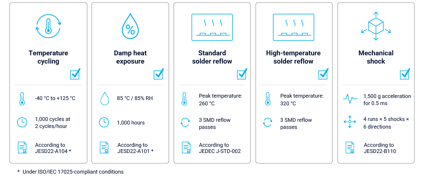
PIC packaging requires materials that offer high optical performance, reliable manufacturability, and long-term stability. Nanoscribe’s photoresins deliver all three characteristics and have been proven to meet stringent assembly and long-term reliability requirements according to JEDEC.
The Nanoscribe Quantum X align enables low-loss coupling across diverse material platforms and component types. With automated alignment, optical components can be printed directly on fibers, chips, and wafers, combining the steps of part production and alignment in one system. With processes optimized for shortest cycle time and highest yield, couplers can be manufactured cost-competitively and at scale.
Fiber-to-PIC coupling
Connect fibers to photonic chips through the chip edge or from above, with optics on one or both components.
Lensed fiber arrays
Print individual lenses on each fiber for parallel connections or contactless wafer-level testing.
PIC-to-PIC coupling
Connect photonic chips across a gap. Lenses printed on both sides guide light from one chip to another.
Laser-to-PIC coupling
Connect lasers to photonic integrated circuits. Lenses adapt the beam to couple light into a waveguide.
Laser-to-fiber coupling
Shape the emitted beam for efficient coupling into a single fiber or fiber array.
Imaging & sensing
Lenses on fiber tips or chips shape and collect light for optical coherence tomography (OCT), endoscopy, and compact sensors.

Aligned 3D printing for integrated photonics & optics
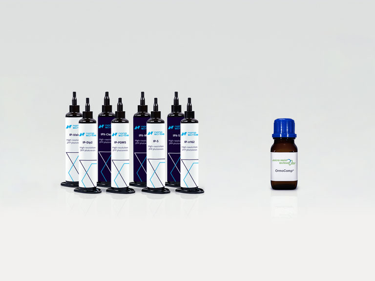
Resins optimized for fabrication of microoptical elements
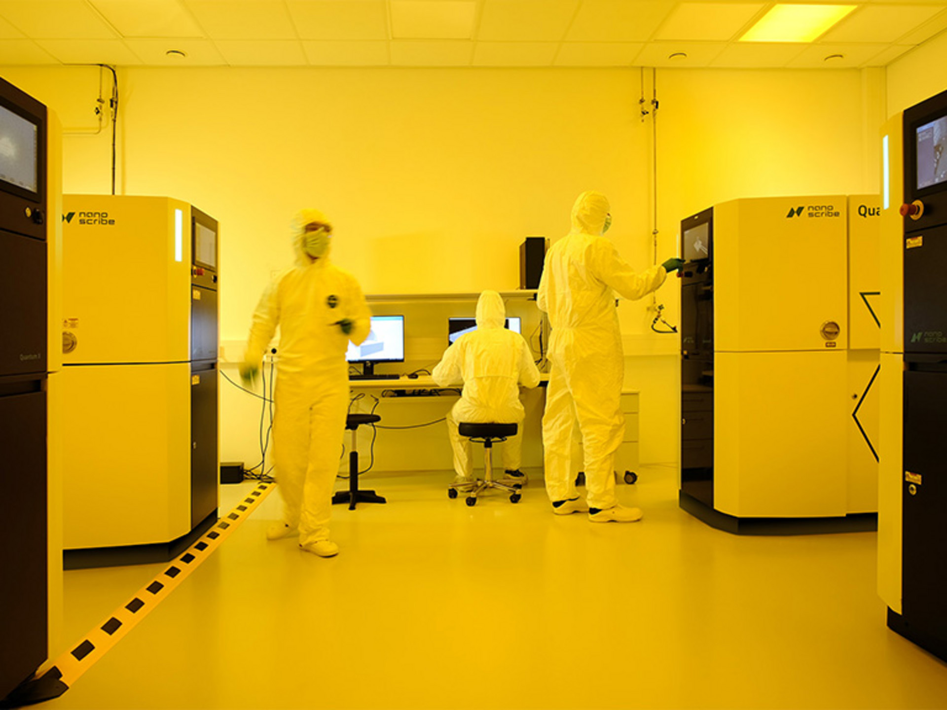
Your guided path to industrial-scale microfabrication
Review your optical coupling interface, alignment requirements, and production goals with our experts – and identify a practical path from feasibility to manufacturing.
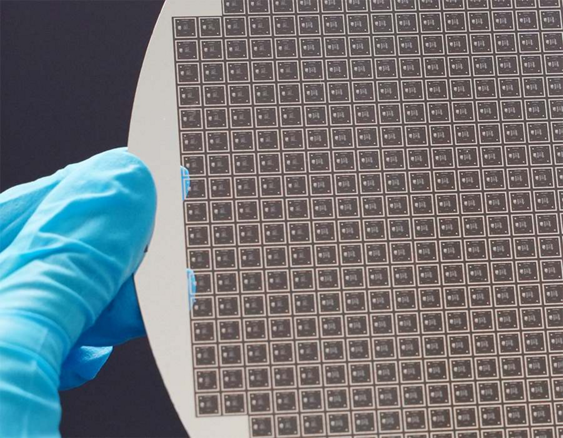
Scaling photonic computing
Explore photonic computing, emerging scaling concepts and high-performance photonic coupling in this webinar.
More info