Applications employing artificial intelligence (AI) pose enormous challenges for electronic hardware in terms of computing power and storage capacity. AI needs processing power growing at a rate of more than five times higher than given by Moore’s Law and this is not possible with current electronic approaches. The PHOENICS project aims to address these challenges with innovative hardware approaches for processing the enormous data volumes, which are needed by demanding AI applications. By moving away from electronic towards photonic approaches, the PHOENICS project will establish disruptive methods for ultrafast information processing.
Photonic integration of different chip platforms
PHOENICS stands for “Photonic enabled petascale in-memory computing with femtojoule energy consumption” and sums up the three goals of the project: In contrast to traditional hardware, the concept of in-memory computing will allow data processing more similar to the human brain by removing the separation between computing and data storage units; photonic technology provides high speed data transport where current electronic systems face severe limitations; taken together, this will lead to a significant reduction of the energy demand.
The PHOENICS information processing architecture is based on the hybrid integration of three different chip platforms: a frequency microcomb chip, which is developed jointly by EPFL and MicroR Systems, an InP (indium phosphide) active modulation unit developed by HHI, complemented with a silicon photonics processor developed by the Universities of Exeter, Oxford, and Ghent. The University of Münster, Nanoscribe and IBM will design the system architecture and join the chip platforms.
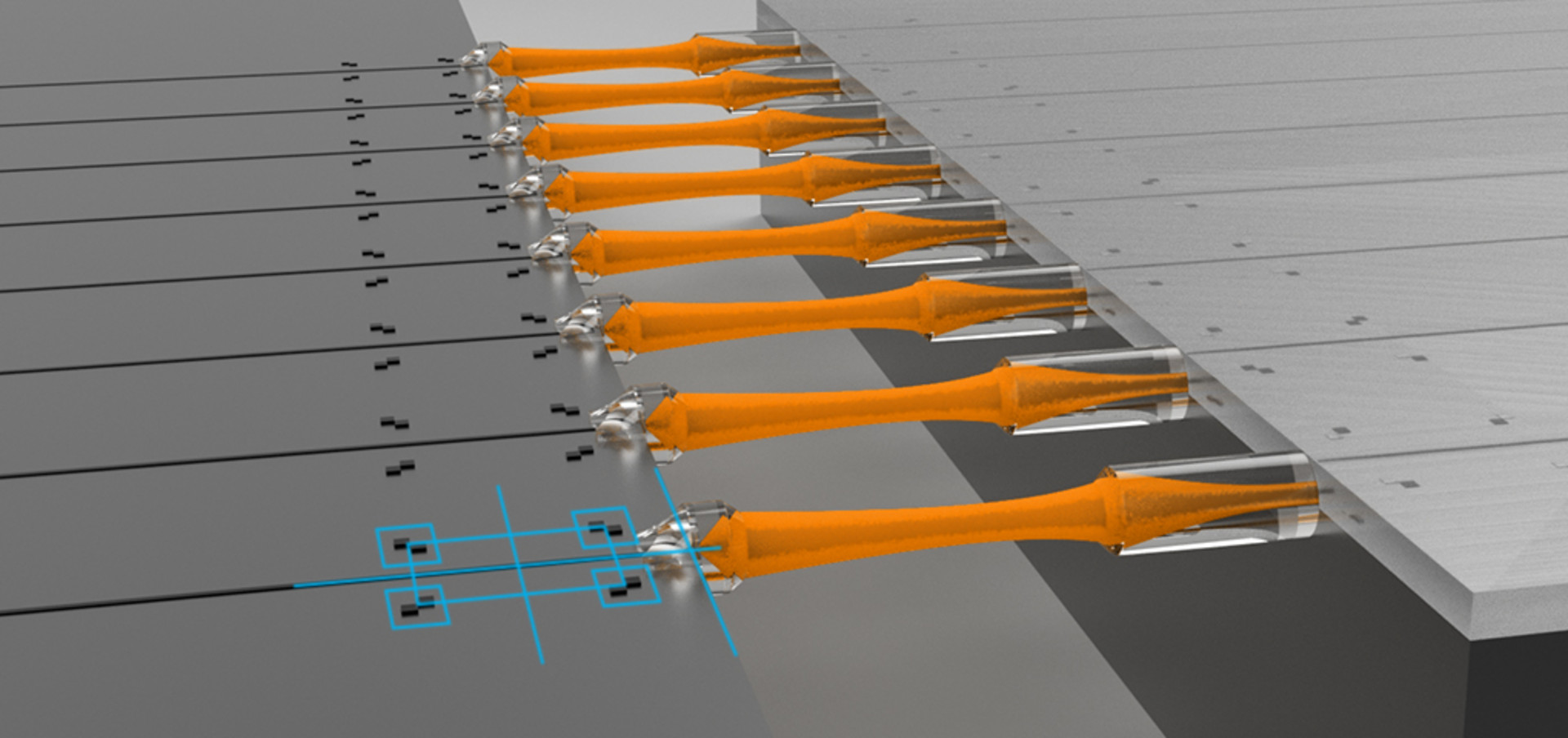
Advances in alignment and packaging of photonic components
In PHOENICS, Nanoscribe will develop new hardware- and software-based solutions for photonics packaging. A key challenge for the industrialization of photonically packaged systems is the wide variety of different photonic platforms which typically all have different optical coupling interfaces. Efficient optical coupling without active alignment thus becomes almost impossible. Nanoscribe intends to integrate the results of the project into complete photonics packaging solutions consisting of automated systems, software, photoresins, and corresponding processes.