Press release
March 25, 2020

Nanoscribe is fully operational at the new ZEISS Innovation Hub @KIT

Karlsruhe.   Nanoscribe has moved into the ZEISS Innovation Hub at the gates of Campus North of the Karlsruhe Institute of Technology (KIT) and now is fully operational. In one of the most innovative high-tech clusters in Germany, the company opens its new headquarters and rolls out extended activities in R&D, streamlined production, customer support, and sales in the brand-new building. The hub offers more than 12,000 m² to intensify the collaboration between business and science, housing the KIT spin-off Nanoscribe together with innovation teams of Carl Zeiss AG, KIT and start-ups in high-tech and digitalization.

Flags of ZEISS, Nanoscribe, KIT in front of ZEISS Innovation Hub

High-tech laboratories, modern production and office space over two floors will drive more innovation and product development in 3D Microfabrication

This January, twelve years after Nanoscribe’s foundation, the award-winning company moved into its new headquarters in the ZEISS Innovation Hub @KIT. Now all laboratories are ready for operation and production has been ramped up. ZEISS and KIT have played a major role for the young company. Nanoscribe is a spin-off of the KIT, whose research and technology ecosystem has strengthened the company as a pioneer and innovator in 3D Microfabrication. And ZEISS has supported and promoted the foundation of the company and subsequently acquired a substantial stake of Nanoscribe.

Sadly, the official building inauguration ceremony had to be postponed in order to enforce the necessary measures to contain the COVID-19 infections. Despite this, Nanoscribe’s facilities and the workforce under this roof are fully operational.

Developing next generation microfabrication

The new headquarters houses facilities to develop and produce the next generation of industrial microfabrication equipment. The premises are equipped with high-tech laboratories, modern production and office areas as well as the Microfabrication Experience Center for the growing company of more than 70 employees and its wide customer base. Within more than 4,200 m² net floor space, high-tech chemistry and physics laboratories have been designed and set up to provide an optimal R&D workspace with best vibration isolation, excellent temperature and humidity stability. The facilities offer the adequate conditions for the development of high-precision additive microfabrication systems with specialized complete solutions that include matching materials, software and processes.

“The ZEISS Innovation Hub offers a very stimulating environment to bring new microfabrication technologies and solutions to the market. Under one roof we have plenty of space, professional equipment and highly qualified employees to develop and manufacture high-precision 3D printers and advanced lithography systems for our customers in science and industry,” explains Martin Hermatschweiler, CEO and co-founder of Nanoscribe. “We are well prepared for coronavirus and the difficult times ahead. We are always personally available for our worldwide customers and we provide comprehensive support with an online knowledge base, webinars, online training options and remote diagnostics and support,” continues Hermatschweiler.

Strengthening collaboration

Nanoscribe works together with high-tech companies and partners from science and industry in various development projects. These efforts focus on key technologies ranging from mobile imaging devices to quantum technologies and integrated photonics, with tremendous impact in health care, automotive and data communications.

“The ZEISS Innovation Hub gives us the space to strengthen local collaboration and attract business and R&D partners from all over the world. The hub brings together multidisciplinary experts from research and high-tech companies to realize advanced microfabrication systems,” states Michael Thiel, CSO and co-founder of Nanoscribe.

Captions

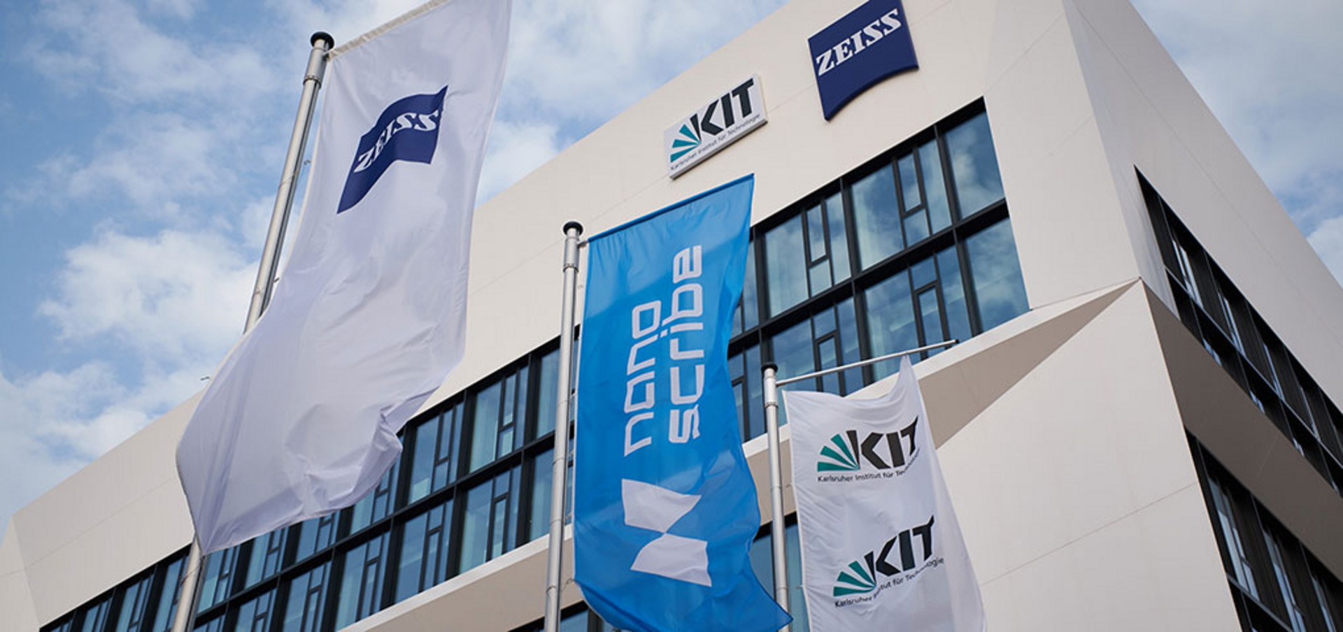
Img. 1: The ZEISS Innovation Hub @KIT houses Nanoscribe together with innovation teams of ZEISS, KIT and high-tech start-ups.
Img. 2: Nanoscribe CEO Martin Hermatschweiler is glad to see that the new headquarters at the ZEISS Innovation Hub @KIT is now fully operational.

Right of use and media relations

Our images may be used free of charge for editorial purposes. Please state the source as follows: "Image: Nanoscribe". The images must not be used for commercial purposes or passed on to third parties.
In case of questions or if you would like to be added to our press mailing list, please do not hesitate to contact Johannes Lang,  lang@nanoscribe.com.

Stay up to date with our latest press releases about Nanoscribe and the world of 3D Microfabrication. Directly get in touch with us to discuss further press activities: Media relations

Login Register
Contact us
Close

It's your choice

Cookies help us to better understand you as a visitor and to provide you with a better experience.

It's your choice
Cookies help us to better understand you as a visitor and to provide you with a better experience.
Legal Notice Privacy Policy
Accept all Individual Settings