
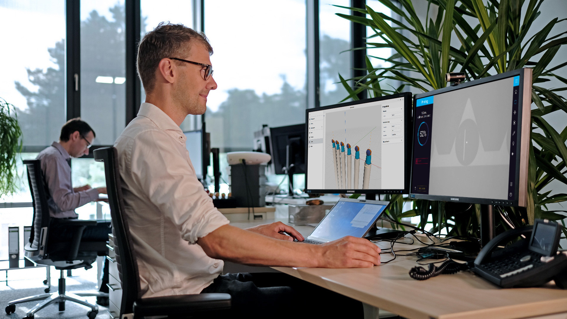
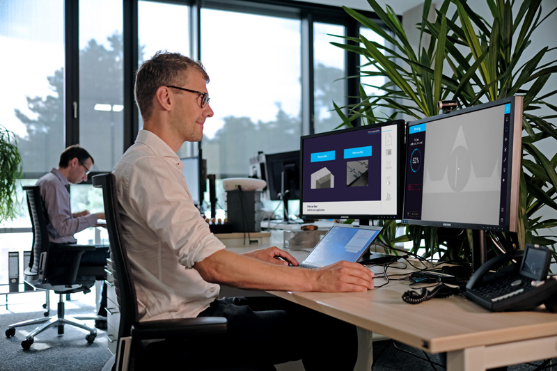
Connect to the photonic world
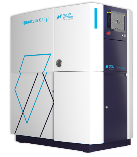
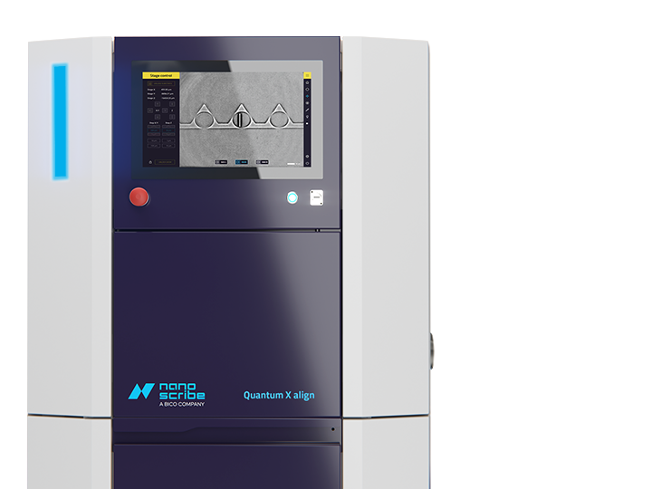
Quantum X align
Aligned 2-Photon Lithography (A2PL®)
drives innovation in photonics packaging
Printing on fibers + chips
Optimized hardware and workflow to print on standard or customized fiber arrays and photonic chips
Nanoprecision 3D alignment
Fiducial and 3D topography detection for 3D alignment on chips and fibers with nanoprecision
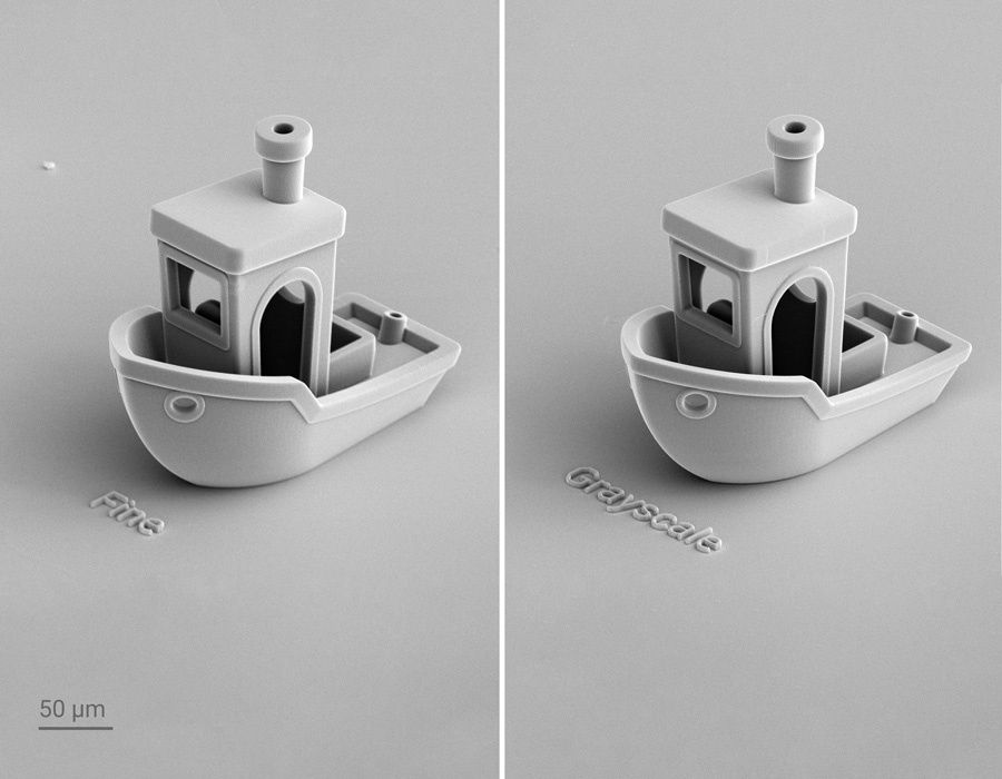
3D printing by 2GL®
New 3D Microfabrication technology with real time voxel tuning for superior quality and speed
3D printing by 2GL®
with nanoprecision alignment system
The Quantum X align with Aligned 2-Photon Lithography (A2PL®) is the fastest and most advanced 3D Microfabrication system of its kind. Nanoscribe’s proprietary voxel tuning technology 2GL® empowers the 3D printing of freeform microoptics precisely aligned to the optical axes of fibers or photonic chips with superior quality and unrivaled speed. These 3D printed microoptics can serve as Free Space Microoptical Coupling (FSMOC) elements for efficient light coupling between photonic components to facilitate photonics packaging or for miniaturized imaging optics.
Align, print, done
Packaging of photonic integrated circuits (PIC) or miniaturized medical devices requires tedious placement and active alignment of the various microoptical elements to each other. Quantum X align simplifies this process: with A2PL optical interfaces on photonic chips or fiber cores and their spatial orientation are automatically detected. Freeform microoptics or diffractive elements are then printed, tilt compensated, directly in place. Thus, the complexity of the process chain is reduced and assembly tolerances are relaxed while enabling even more compact devices. The often costly active alignment is no longer necessary.
Align to optical fibers and photonic chips
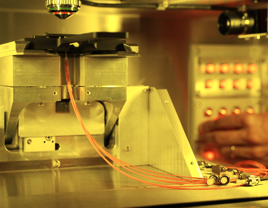
A fiber illumination unit, in conjunction with smart software routines such as automatic tilt compensation, ensures precise alignment onto single cleaved fibers or v-groove fiber arrays. Automated detection routines ensure lowest coupling losses and highest repeatability.
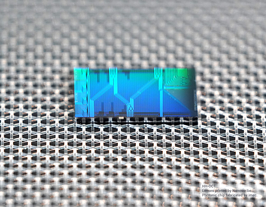
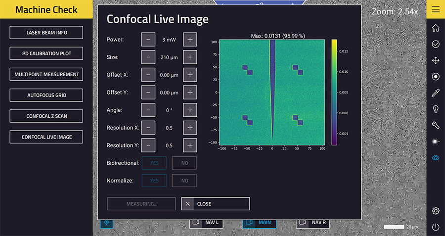
Quantum X align also features a confocal detection module for 3D topography detection and fully automatic 3D alignment to fiducials via pattern matching. This makes Quantum X align the ideal tool for 3D printing microoptical elements directly onto surfaces and facets of photonic chips, and thus for photonics packaging processes.
Align to your ideas
The Aligned 2-Photon Lithography technology with nanoprecise 3D alignment, coupled with a powerful and user-friendly workflow, also opens up new opportunities for 3D Microfabrication beyond microoptics. From microfluidics to complex sensor systems or MEMS: Quantum X align is the perfect two-photon lithography tool for high-precision direct laser writing, automatically positioned with highest precision onto complex 3D substrates, even on tilted or angled structures.
Technical features in brief
- High-performance 3D Microfabrication by Aligned 2-Photon Lithography (A2PL®)
- 3D printing by 2GL® Two-Photon Grayscale Lithography providing superior quality at unrivaled speed
- Powerful software nanoPrintX for 3D printing with precise alignment to fiber cores and fiducials on chips and other substrates
- Fiber illumination unit for fiber core detection ensures precisely aligned printing to the optical axes of fibers
- Confocal detection module for 3D substrate topography mapping enables precisely aligned printing on the surface and facet of chips
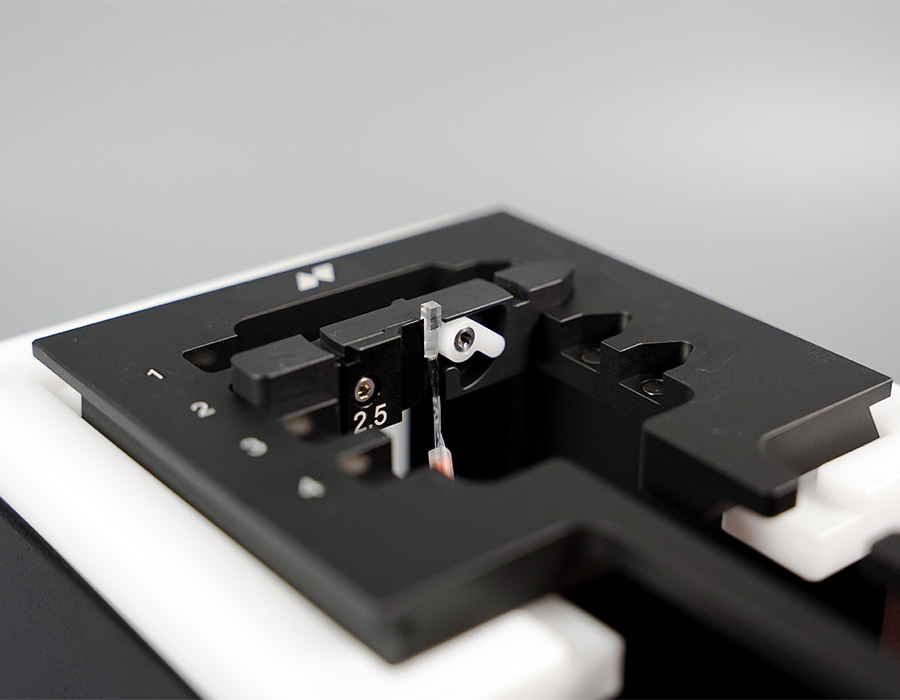
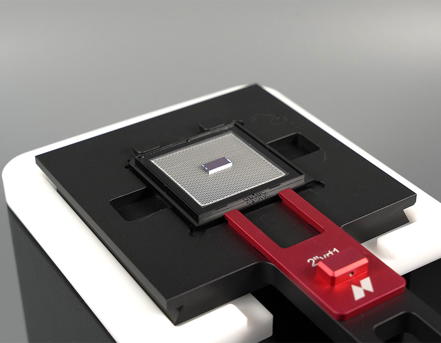
- Proprietary substrate holders for fibers, fiber arrays and photonic chips
Printing processes and workflow
- High-precision 3D printing based on Two-Photon Polymerization (2PP)
- Aligned 2-Photon Lithography (A2PL®) for printing of structures relative to fiducials or on fiber facets
- 3D printing by 2GL® for stunningly fast and accurate printing of any freeform design
- Easy and robust setup with Dip-in Laser Lithography (DiLL)
- 3D alignment detection accuracy down to 100 nanometers
- Feature size control down to 100 nanometers
3D printing by 2GL® for
superior quality at unrivaled speed
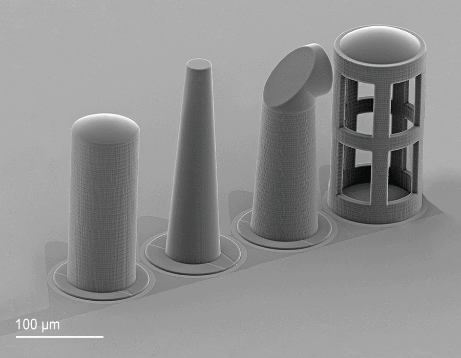
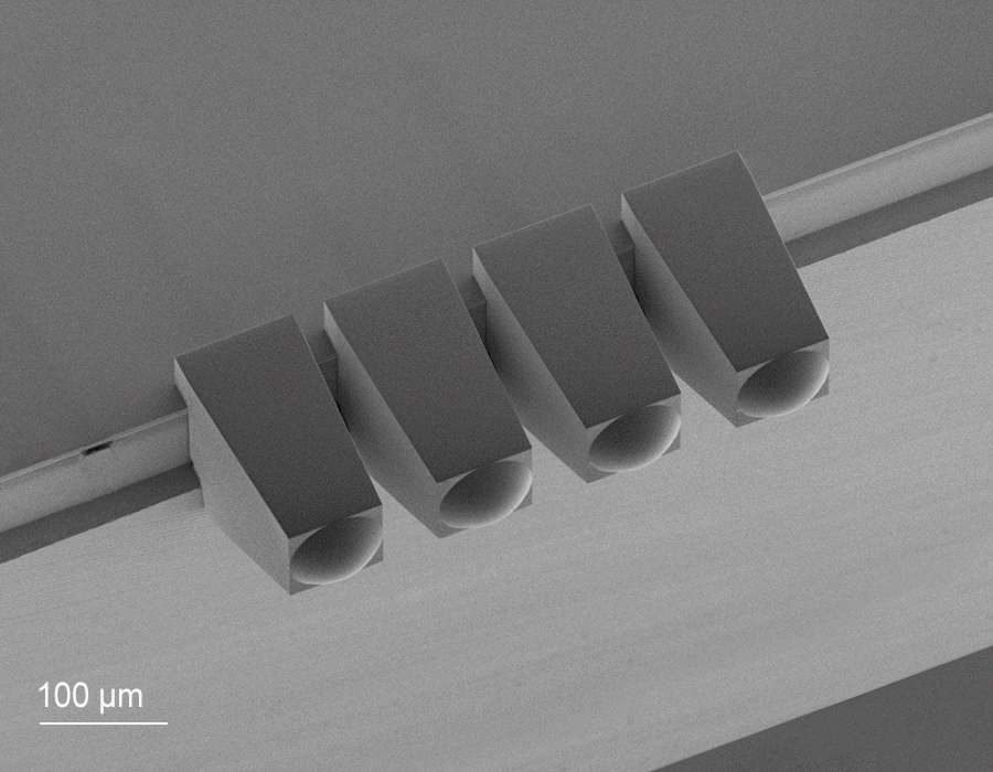
Quality and speed! No more compromises, thanks to our patented voxel tuning technology: 3D printing by 2GL® Two-Photon Grayscale Lithography sets new standards in 3D Microfabrication. Print any 3D shape using the fastest nanoprecision additive manufacturing technology on the market. Are you ready for truly outstanding print results?
Unmatched precision
with outstanding shape accuracy
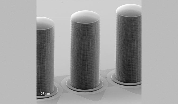
3D printing by 2GL® takes Nanoscribe’s grayscale technology to the third dimension. The printing process relies on dynamic modulation of laser power in real time while scanning at highest speed. This results in a precise size adjustment of the polymerizing voxel to perfectly match the contours of any 3D shape. Your result: Flawless, optical-grade surfaces, no slicing steps, no shape distortion, just the real shape of any 3D print design.
Up to 60 times higher throughput
3D printing by 2GL® is the fastest 2PP-based microfabrication technology on the market. Its dynamic voxel tuning requires significantly fewer printing layers to achieve print results with optical-grade, smooth as well as nanostructured surfaces. This translates to a manufacturing speed unattainable by any 2PP-based 3D printer available.
Take advantage of 2GL® as the fastest additive manufacturing technology on the market for 3D nano- and microfabrication, with 10 to 60 times the throughput of any current 2-photon lithography system when meeting demanding print quality requirements.*
* Comparison refers to the same print quality and is design-dependent
Connect to the photonic world
Facts and figures on Quantum X align
- High-performance 3D printing of microoptical elements onto optical fibers and chips by A2PL® technology
- 3D printing by Two-Photon Grayscale Lithography (2GL) with superior quality at unrivaled speed
- Smart slicing for optimized resolution, precision and speed
- Automatic 3D alignment system with nanoprecision in all spatial directions
- High-precision fiber core detection based on fiber illumination unit
- 3D mapping of substrate topographies by confocal detection module
- Define structure placement relative to fiducials on chips and other substrates using nanoPrintX software
- Automatic substrate tilt recognition and print adjustment
- Substrate holders for fibers, fiber arrays and photonic chips
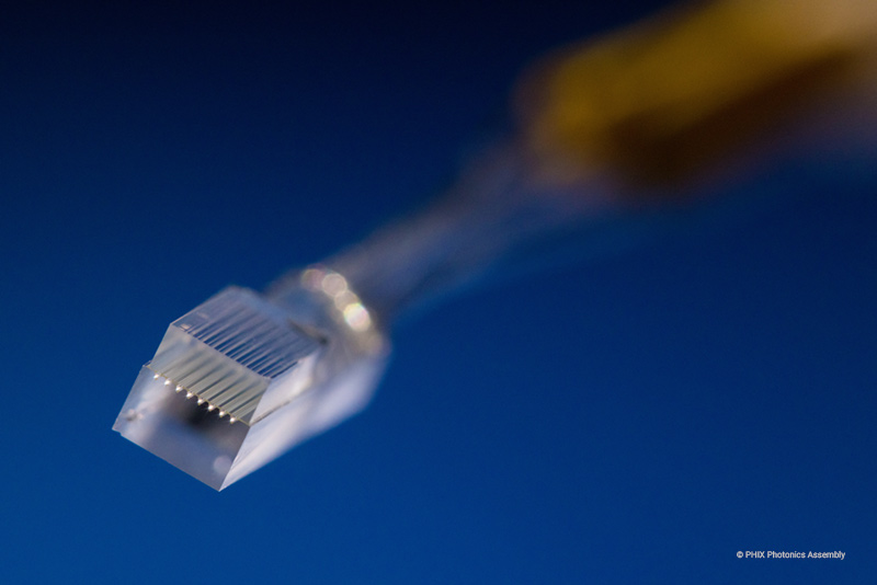
Rapid prototyping and small series production of precisely aligned freeform microoptics
- Lensed fiber arrays for optical interconnects
- Imaging and beam shaping optics on single fibers or fiber arrays
- Free space microoptical couplers
- Beam shaping or light collection on photonic chips
Designed for pioneers and innovators in research and industry active in
- Integrated photonics
- Photonic packaging
- Medical instrumentation
- Optical sensing
- Quantum technology
Benchmark scores
| 3D alignment detection accuracy 1 | down to 100 nm (xy) / 500 nm (z) |
| Surface roughness Ra | down to ≤ 10 nm |
| Shape accuracy Sa | down to ≤ 200 nm |
| Feature size control 2 | down to 100 nm |
| Typical processing time | 10 min. for 8x lensed fiber array |
| Achievable coupling losses 3 | down to ≤ 1 dB |
General system properties
| Printing technology | Aligned 2-Photon Lithography (A2PL®) |
| Substrates | Fiber arrays (v-groove) |
| Photoresins | Nanoscribe IP Photoresins (polymers printing) |
| Maximum print area | 50 x 50 mm² |
Peak values, only achieved under specific conditions such as printing parameters, print heads, photoresins, and designs.
Given values may vary depending on the photoresin and structure geometry.
1 With confocal detection. Accuracy depends on selected print head
2 100 nm feature size control in x/y direction
3 Best case for typical applications, depending on design, substrate quality and measurement method
Joost van Kerkhof, Chief Operations Officer of PHIX Photonics Assembly

We are confident in Nanoscribe’s new, aligned 3D printing technology for producing lensed fiber arrays and lensed chips with virtually limitless optical designs.
Set the scene with nanoPrintX
Compose and align your prints smarter
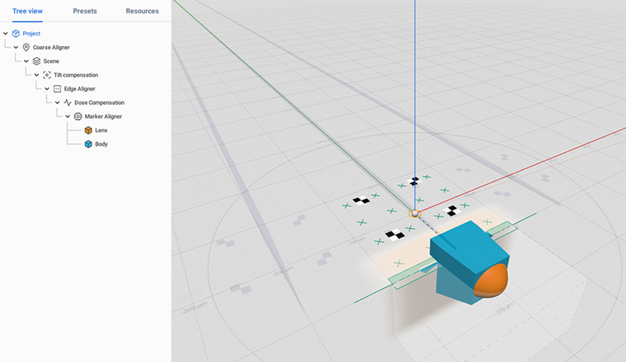
nanoPrintX is much more than a 3D printer slicer software. It is a game-changing tool to create sophisticated print projects for aligned 3D printing, supporting our revolutionary 2GL-technology. The underlying scene graph concept, a tree-like data structure that provides a hierarchical organization of all print-relevant objects and operations, enables an agile definition of what, where, in which spatial orientation and how to print. The intuitive software architecture, combined with a central rendering canvas, provides instant visual feedback on the position and spatial alignment of all elements relative to each other and to predefined positions or substrates.
Each node of the nanoPrintX scene graph is a print-relevant object or operation and includes a set of adjustable properties. You can import several design files and organize them into group or array nodes, or merge multiple files into one print object. To make the most out of the Aligned 2-Photon Lithography (A2PL) technology, you can define individual alignment markers as well as substrate features such as chip edges and fiber facets. Using Quantum X align's confocal unit or fiber illumination unit, these specific substrate markers can be identified and matched to the digital model defined with nanoPrintX.
Compose your print project with nanoPrintX: Define the print scenario by creating a virtual model of your specific substrate, such as optical fibers or photonic chips with individual alignment markers. Import your 3D print designs as STL or OBJ files and place them into your scene. Assign pre-developed print parameters to individual designs as needed, and they work right out of the box. Get the most out of your design with the brand new presets for 3D printing by 2GL®. Finally, simply upload your print project to Quantum X align and enjoy the results.
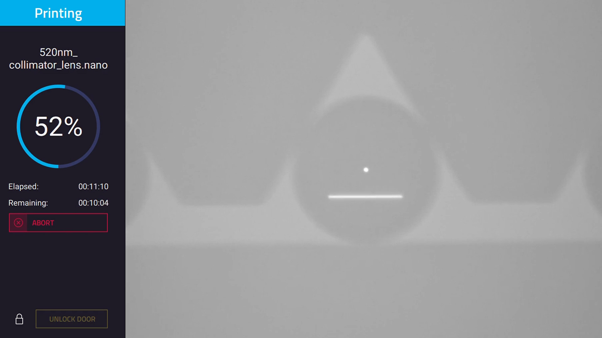
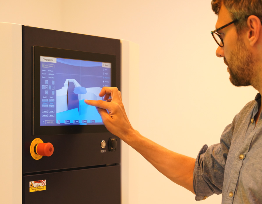
Start your print project via the touchscreen: The intuitive touchscreen user interface of Quantum X align easily guides you to successful printing. Register the starting positions on each substrate, double check using the high-resolution live camera view and start your print project. The system will then automatically align your prints with respect to your markers with submicron accuracy.
Stay connected with nanoConnectX: Start and monitor your print project from the office with the remote access software nanoConnectX. It brings all the control functions and display capabilities of Quantum X align’s front panel touchscreen to any computer connected online. The Quantum X align system is hereby well equipped for production environments and multi-user scenarios.
Software facts
nanoPrintX is a print project development software based on scene graphs. With this modern, tree-like data structure, you can easily generate logical relationships between elements of the print and assign individual properties or print parameters. This allows you to exactly define how the printed structures are aligned to the substrate and to each other.
Load multiple CAD designs into one scene and assign different print parameters to each part design. This allows you to fine-tune your print for optimized quality and speed for each section. With the combination of the new 3D printing by 2GL® technology and the smart slicing feature with coarse speed print parameters, optical elements can be printed up to 60 times faster. Many actions can be dynamically configured using drag and drop.
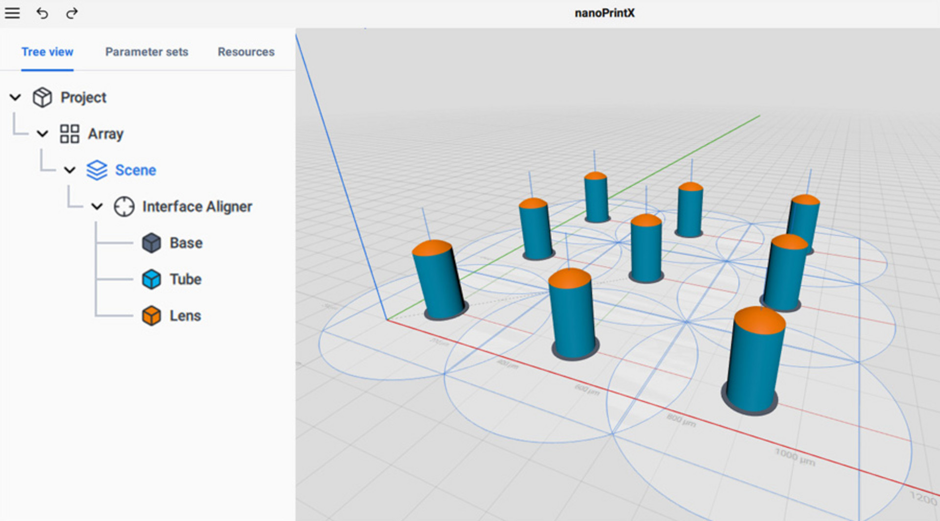
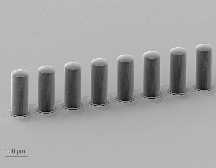
With nanoPrintX you can design your individual Lensed Fiber Arrays (LFAs) in just a few steps.
Select the fiber node in the scene graph and place your individual lens designs as .STL or .OBJ files on the fiber. With just a few steps you can easily generate multiple copies of the same print or customize each fiber with an individual design.
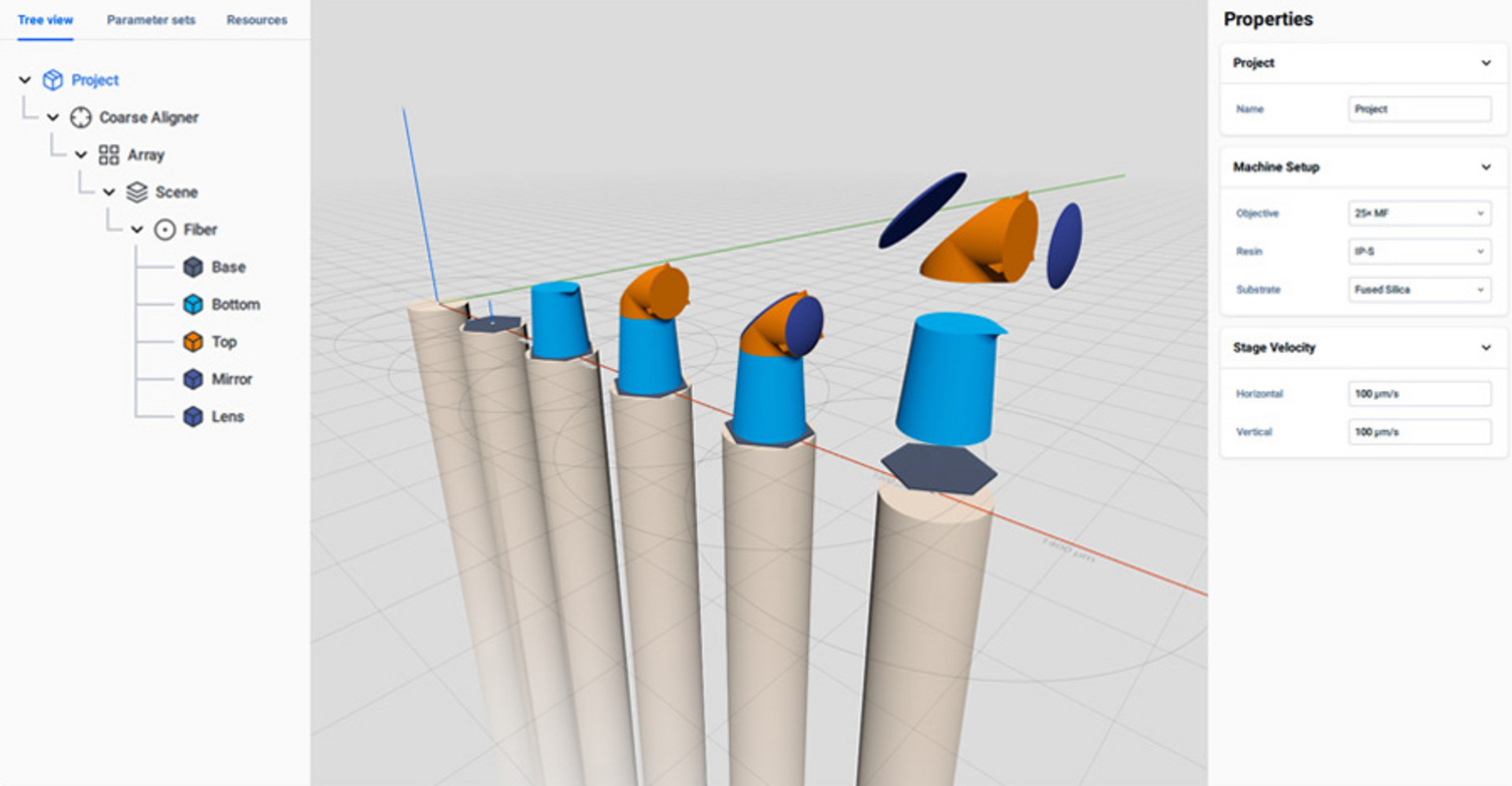
Design your prints for high-performance microoptical elements at the interface of photonic chips. With nanoPrintX, alignment markers can be easily applied to your chip layout, loaded as image files, and automatically matched to the alignment markers on your chips during printing. Place the CAD designs of your printing objects relative to the alignment markers and assign pre-defined printing parameters to each element of the print. Intelligent alignment features such as edge detection and dose compensation lead to flawless printing results, even in challenging printing scenarios such as at the edge of photonic chips.

Control and monitor the system with nanoConnectX, the remote access software for the Quantum X platform. It guides you to a successful print in just a few steps.
Select your print project, register the starting position and start printing. The system then automatically aligns and prints the structures in exactly the right position and spatial orientation.
Making opportunities happen with new features
Check out how
3D-aligned nanofabrication comes about...
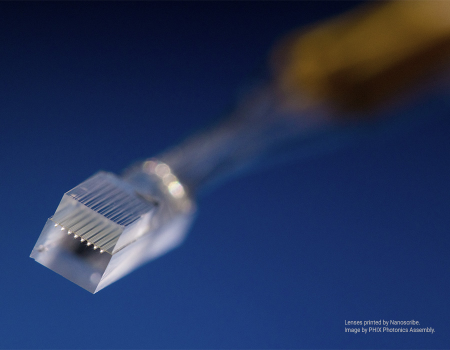
How does aligned printing on the facet of optical fibers work?
With the fiber illumination unit, the fiber core can be easily located using the Quantum X align touchscreen. First, the print field on the fiber array is defined by manual coarse alignment with a double-tap on the touchscreen. Then, Quantum X align automatically detects the position of the fibers with submicron accuracy and compensates for smallest substrate tilts during the print in all spatial directions.
For this, the autofocus routine first detects the surface of the optical fiber. Next, the system identifies the illuminated fiber core and marks the center of the core as the origin of a virtual coordinate system to which the print object is aligned. The virtual z-axis and its orientation in space is determined by moving the substrate downwards and identifying the position of the fiber core on multiple positions along this vertical movement of the stage. As a result, the optical axis orientation is detected and set as the virtual z-axis for a tilt compensated printing of microoptics with submicron precision.
What role does hardware play in the fiber printing workflow?
To support the fiber printing workflow, Quantum X align is equipped with a red LED fiber illumination unit. Up to 32 individual fibers with standard PC or APC connectors can be plugged into this unit. The specially designed fiber substrate holder secures single fibers or fiber arrays and can load up to four fiber arrays at a time. Once inserted into the printer, the illuminated fiber cores can be easily identified using the live microscope view on the 18.5-inch touchscreen of Quantum X align. A double tab on the screen allows the stage to be moved to any position within the 50 x 50 mm² print area. A crosshair can be activated to facilitate the rough alignment on the screen, and intuitive gestures let you zoom in and out on the screen.
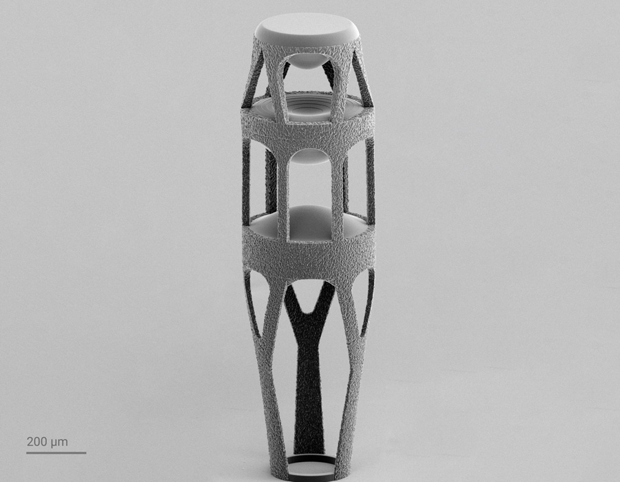
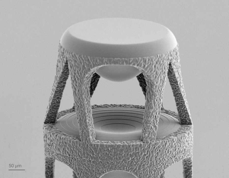
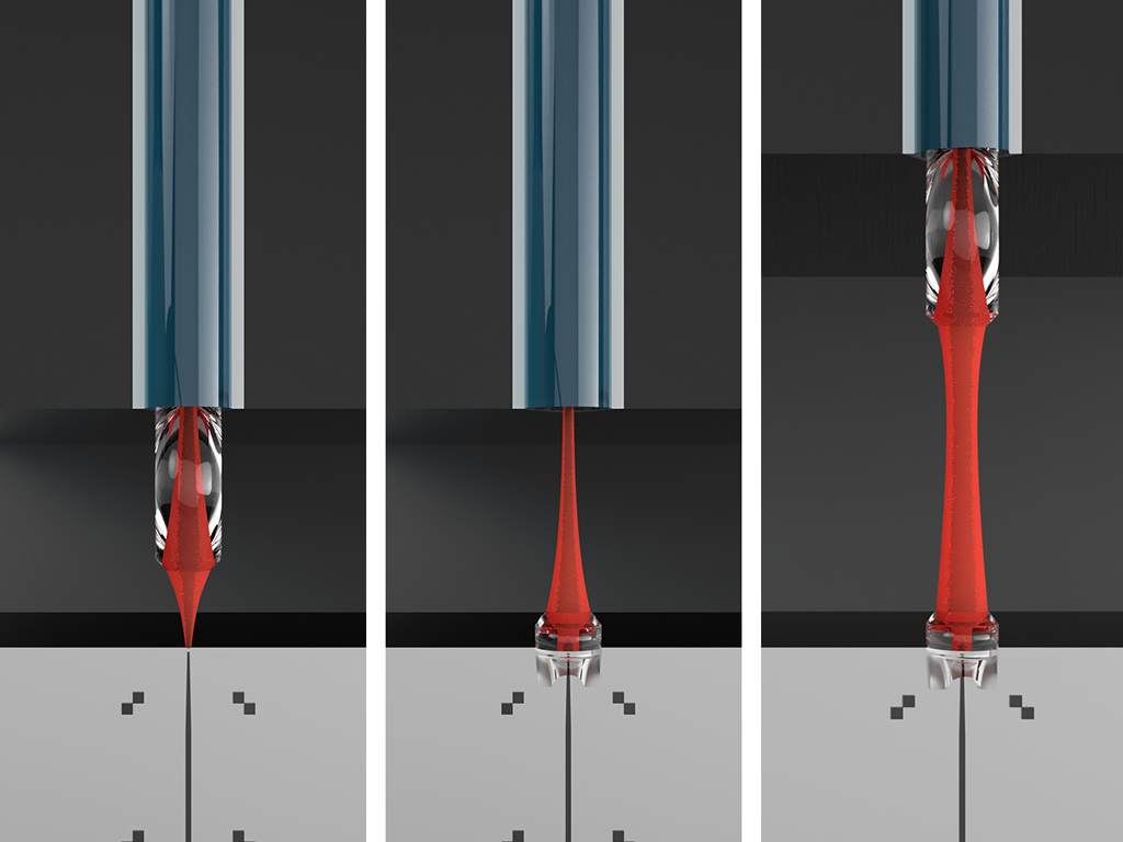
How can complex objects with optical quality surfaces be printed at the highest speed?
The new workflow can load multiple .stl or .obj files and merge them to one single print object. This enables the user to set individual print parameters, such as slicing, hatching, laser power or scan speed, for each individual part of the print object. As a result, support structures can be printed faster with coarse parameters, whereas optical parts such as the surface of a lens can be printed with finer settings that result in a surface roughness (Ra) of 10 nm and even less. Of course, predefined print parameters are available out of the box but can also be customized to fit the design and specific requirements. The individual parts are then merged to one print project and uploaded to Quantum X align.
Adjusting print parameters to the functional requirements of the print object saves valuable process time and enables Quantum X align to process an 8x V-groove fiber array in less than 20 minutes.
Why is a confocal unit used for automatic topography alignment?
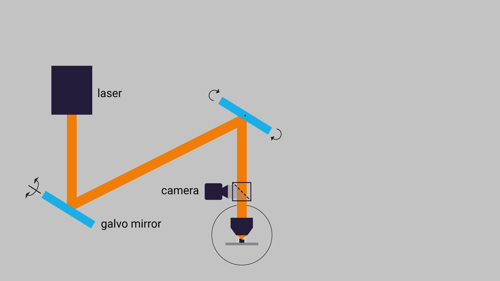
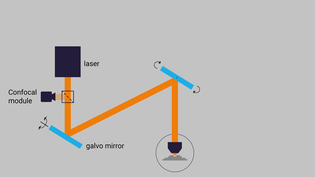
Quantum X align features a high precision confocal imaging module for 3D mapping of substrate topographies. This module is integrated into the beam path of the near-infrared printing laser. The laser beam is scanned over the sample surface and the back-scattered light is confocally detected by the system. High resolution 3D topographies are recorded by moving the stage vertically and repeating surface scans multiple times along the z-axis. A spatial filter pinhole in front of the detector ensures that only light from the focal plane is detected, resulting in a lateral detection accuracy down to 100 nm. Thus, the confocal module measures real 3D topographies and is more precise than image-based measurements using the system camera.
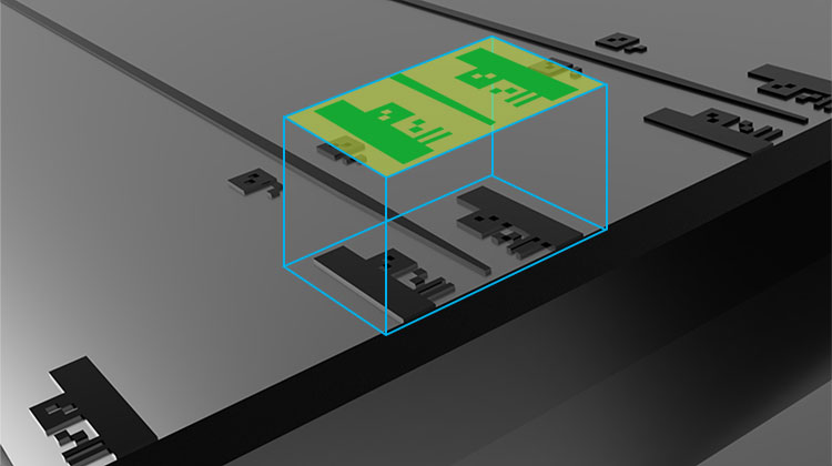
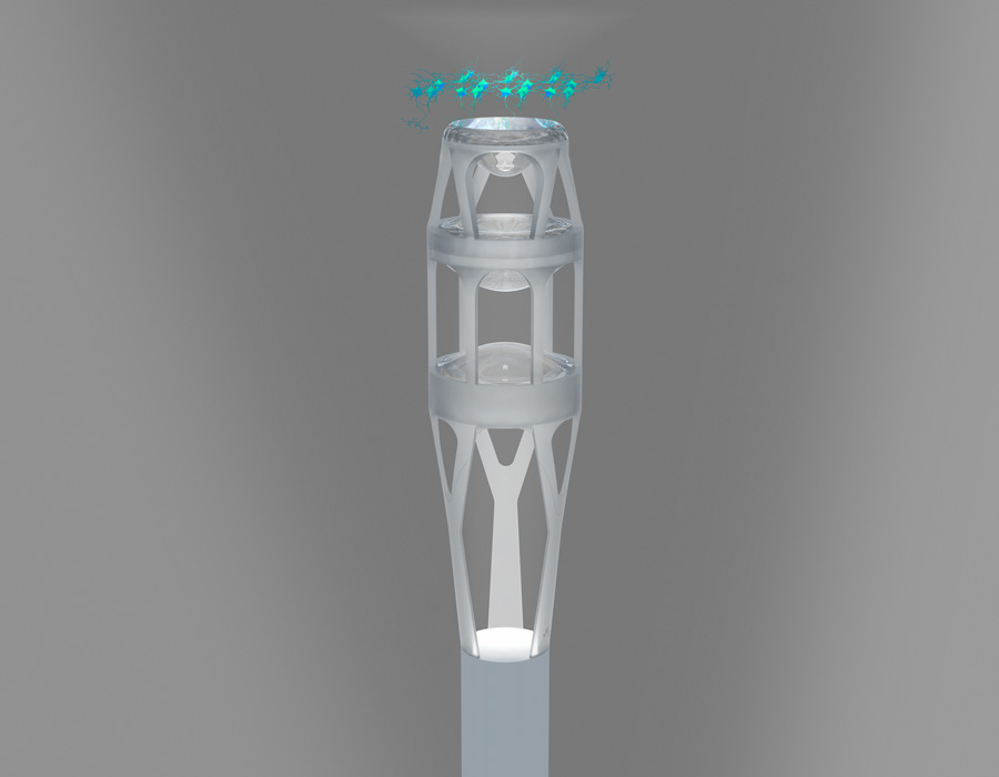
How are optical components aligned and printed onto a photonic chip?
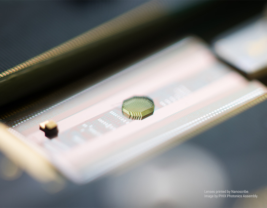
The 3D alignment of the print object is based on the high-resolution 3D topography mappings by the confocal unit. For the precise alignment of optical components on a photonic chip, smart software algorithms automatically identify predefined markers and topography features. Thus, the exact position and orientation of the waveguides on the chip can be determined. A virtual coordinate system is then set to the exit of the waveguide, perfectly aligned with its optical axis and orientation. The desired optical components are printed with respect to this coordinate system, ensuring best optical performance and minimizing coupling losses. This enables efficient light coupling by Free Space Microoptical Coupling (FSMOC).
How does Quantum X align overcome the challenges of printing on the facet of photonic chips?
Printing onto a chip’s facet from top, i.e. perpendicular to the substrate surface, is a challenging task and requires not only a precise positioning system but also smart solutions to overcome the “shadowing effect”: When printing onto a facet, a substantial part of the intensity in the focal point of the printing laser is lost, because the light is partly blocked by the edge of the substrate. Close to the substrate wall the shadowing effect is more prominent and requires higher exposure doses.
For printing aligned onto the facet of a chip the Quantum X align uses a confocal module to detect the edge of the chip and automatically adjusts the laser power during printing with a proprietary dose compensation feature. As a result, microoptics and other print objects are printed onto the facet of a substrate with submicron accuracy.
What range of different substrates can be used?
Nanoscribe’s substrate holders guarantee a precise fixation and enable to print on the facet of single fibers, fiber arrays and photonic chips. Furthermore, standard substrates such as microscope slides and wafer formats from 1” to 6” can be easily processed. The advanced interface finder of Quantum X align includes two complementary modes for reflection and fluorescence detection of the substrate surface. In combination with the Dip-in Laser Lithography (DiLL) configuration, a wide range of reflective (e.g. silicon wafers), transparent and opaque substrates (e.g. glass and polymer substrates) can be used.
What are the unique advantages of the proprietary Dip-in Laser Lithography (DiLL)?
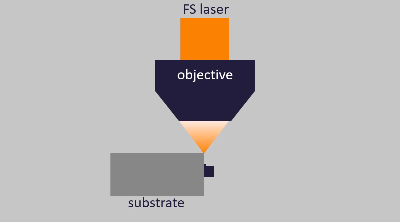
Dip-in Laser Lithography (DiLL) is the standard printing configuration of Quantum X align. Nanoscribe invented this technology for 3D Microfabrication with the highest precision and the lowest aberration on the market. In this configuration, the objective lens is immersed in the photoresin, which also serves as an optical immersion medium. The refractive index matching between the focusing optics and the print material guarantees ideal, aberration-free focusing with the highest resolution in 2PP-based 3D printing. Furthermore, the writing laser is not focused through the substrate (e.g. oil immersion configuration), but writes the print object directly onto the substrate. Consequently, the working distance of the focusing optics does not limit the height of the 3D-printed object, which is especially beneficial for printing macroscale objects.
Why is it so easy to integrate Quantum X align into production environments and multi-user facilities?
The advanced autofocus system reliably finds the interface of any substrate with maximum accuracy and repeatable print results. Three live-view cameras facilitate process control and monitoring. An automatic dispenser applies the correct amount of photoresin onto the substrate, reducing workload and enabling remote operation. To simplify switching between hardware configurations, the Quantum X align automatically detects the printheads and substrate holders. Quantum X align software controls and monitors print jobs in real time and supports intuitive operation through an interactive touchscreen control panel, or remotely from the office via the remote access software nanoConnectX. This remote access also simplifies the work of entire user groups, e.g. members of a research group or a department, with a single or multiple systems, each of them accessing the Quantum X align from their own computer.
What site conditions do our devices need for optimal operation?
Quantum X align is the ideal tool for high-speed 3D Microfabrication of objects with submicron feature sizes, surface roughness profiles of 5 nm and less and nanoscale precision. This highest precision in 3D printing can only be exploited to the maximum by taking some precautions with regard to the system itself and the installation site. Quantum X align should have its fixed place in a room with stable room temperature and humidity. The printer comes with a heavy granite base to reduce the influence of vibrations and temperature fluctuations of the environment. Nevertheless, it is important to install the high-precision printer in a location that minimizes external vibrations. For the handling of the UV-sensitive photoresin outside the printer, we recommend to equip the room with yellow light and to meet basic requirements of a chemistry lab to handle organic solvents for the print development process properly.
If you would like to get an idea of how the Quantum X align work environment can look like, contact us and visit our Microfabrication Experience Center here at Nanoscribe or book your online tour.
How does Free Space Microoptical Coupling contribute to advancing the development of photonics packaging?
Free Space Microoptical Coupling (FSMOC) offers a highly robust and efficient light coupling solution for photonic packaging and integration. Freeform microoptics fabricated directly on the optical interface of chips or fibers enable tailored beam shaping and mode field adjustments. This leads to relaxed alignment tolerances between optical elements and eliminates the need for active alignment, e.g. for fabricating optical interconnects. FSMOC is flexible in use and can be easily tailored to meet application specific requirements. Even previous mode field adjustments at the chip level can be transferred to the new 3D printing approach.
- Cost efficient photonics packaging strategy
- Relaxed alignment tolerances for passive alignment
- Achievable coupling losses down to ≤ 1 dB
- Easy and quick adaption to new requirements and applications
Quantum X align
Connect to the photonic world
Aligned 3D printing.
We would be pleased to prepare a customized offer for you.
For this, please clarify the details with our sales experts.
Interested in validating our technology and products for your projects? Schedule a Quantum X align product demo or book a feasibility check of your design.